Plasma etching method and semiconductor device manufacturing method

a technology of etching method and semiconductor device, which is applied in semiconductor/solid-state device testing/measurement, semiconductor devices, electric discharge tubes, etc., can solve the problem of becoming increasingly difficult to ensure the uniformity of etching rate in the wafer plan

Active Publication Date: 2014-08-21
TOKYO ELECTRON LTD
View PDF3 Cites 268 Cited by
  • Summary
  • Abstract
  • Description
  • Claims
  • Application Information

AI Technical Summary

Benefits of technology

[0009]According to an aspect of the present invention, a plasma etching method may be provided that can achieve uniformity in the etching profiles of via holes and trenches within a wafer plane.

Problems solved by technology

As the wafer hole diameter is enlarged, it becomes increasingly difficult to ensure in-plane etch rate uniformity within a wafer plane.

Method used


Image

  • Plasma etching method and semiconductor device manufacturing method
  • Plasma etching method and semiconductor device manufacturing method
  • Plasma etching method and semiconductor device manufacturing method

Examples


first embodiment

[0044]In the following, a first embodiment of the present invention is described with reference to the accompanying drawings.

[0045](Plasma Etching Apparatus Configuration)

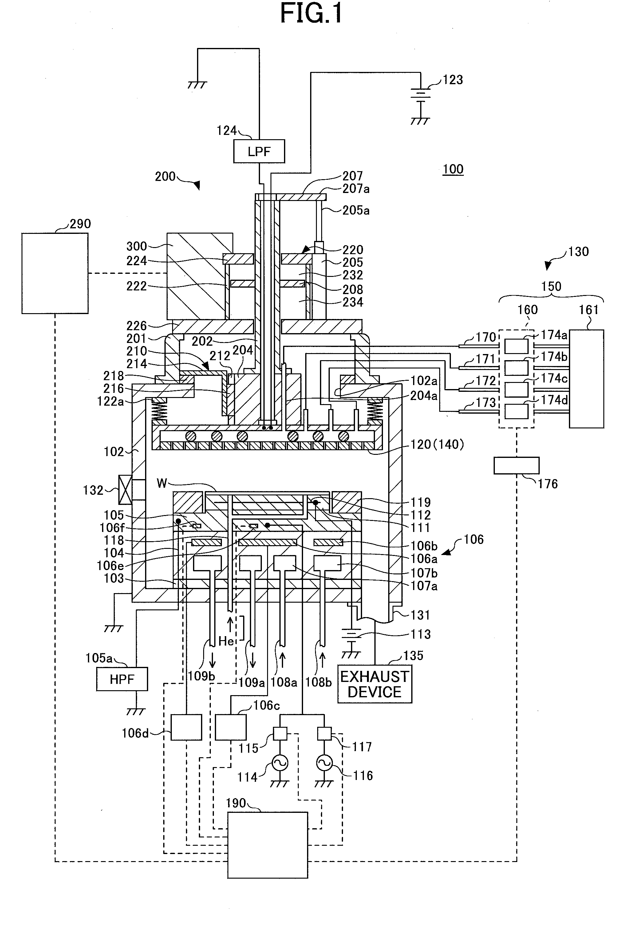
[0046]First, referring to FIG. 1, a plasma etching apparatus 100 that may be used for implementing a plasma etching method according to the present embodiment is described.

[0047]As illustrated in FIG. 1, the plasma etching apparatus 100 of the present embodiment includes a cylindrical chamber (processing chamber) 102 made of aluminum having an alumite-treated (anodized) surface, for example. The chamber 102 is grounded.

[0048]A substantially cylindrical susceptor support 104 is arranged at a bottom portion within the chamber 102 via an insulating plate 103 made of ceramic, for example. A susceptor 105 corresponding to a lower electrode is arranged on the susceptor support 104. The susceptor 105 is grounded via a high pass filter (HPF) 105a.

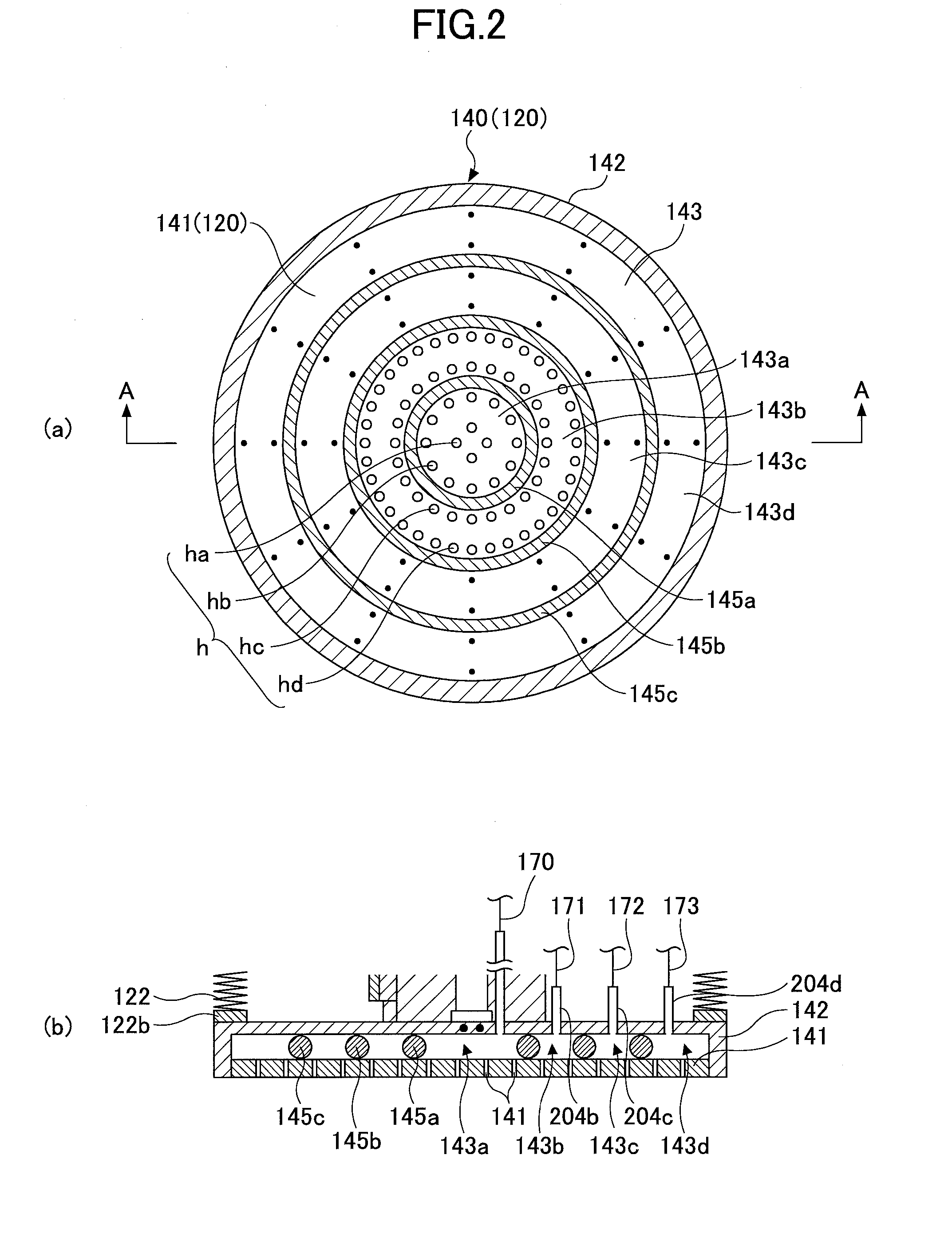
[0049]The susceptor 105 has an upper side center portion arranged into a con...

second embodiment

[0140]In the following, a second embodiment of the present invention is described with reference to the accompanying drawings.

[0141]As described above, in plasma etching, a gas containing fluorine, chlorine, and oxygen, for example, may be used as an etching gas that is turned into plasma. Plasma includes active species such as charged particles (referred to as “ion” hereinafter) and neutral particles (referred to as “radicals” hereinafter), for example. The surface of a wafer reacts with the ions and radicals contained in the plasma to prompt the generation of reaction products, and etching of the wafer progresses as the reaction products are volatized.

[0142]In recent years, there is an increasing demand for forming holes with larger diameters in a semiconductor device manufacturing process, and as a result, it is becoming increasingly difficult to ensure in-plane etch rate uniformity. Techniques are known for improving in-plane uniformity within a wafer by controlling the density ...
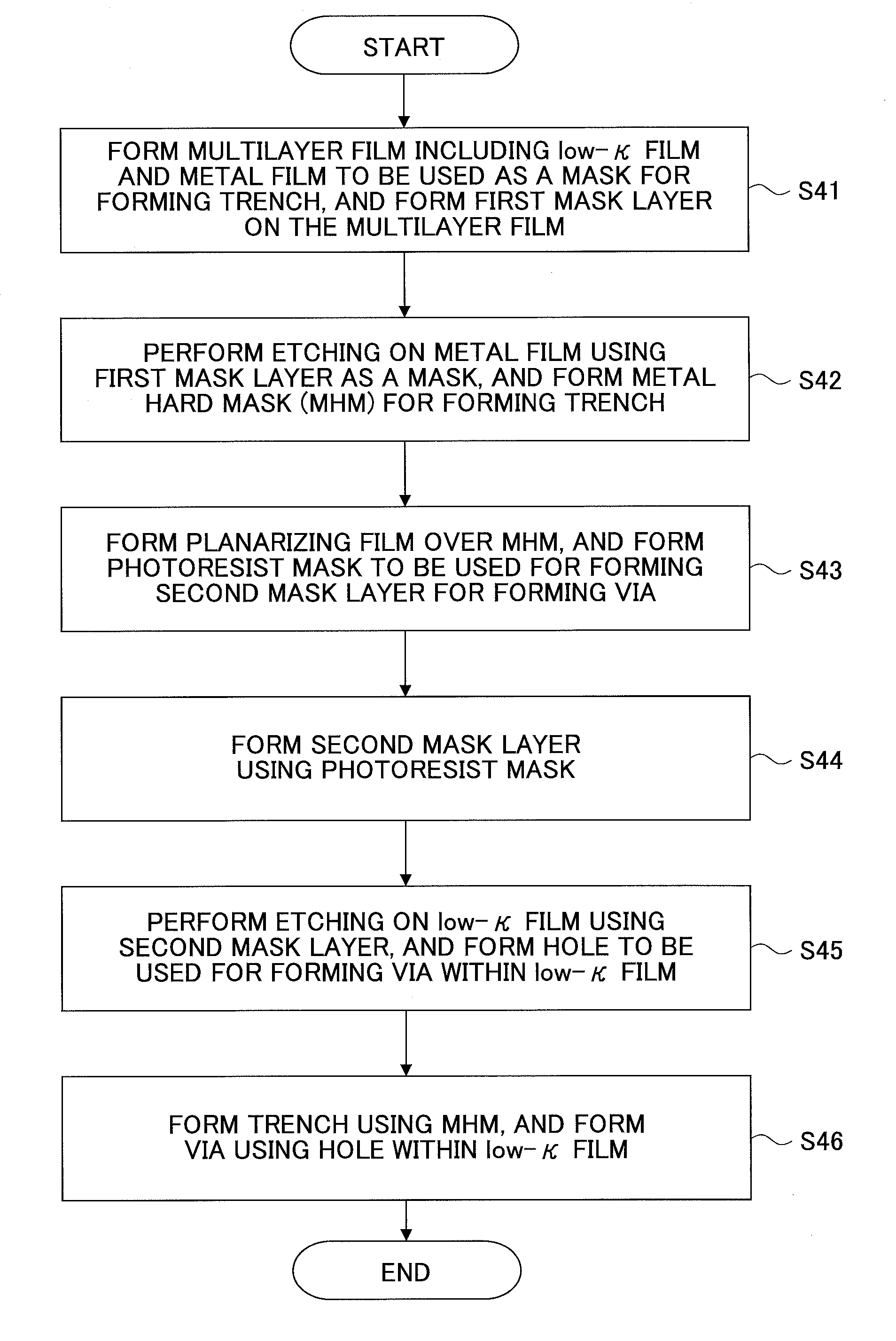
experiment 1

[0243]First, a wafer (300-mm-diameter wafer) having a low-κ film, a silicon oxide film, and a TiN film formed thereon in this order was prepared. These films were formed according to the method described above with reference to FIG. 10 (a). Then, a photolithography process and an etching process were performed to arrange the TiN film into a line pattern and form a metal hard mask (MHM). Then, the silicon oxide film exposed at an opening of the MHM and the low-κ film beneath the silicon oxide film were etched by a C4F8 / Ar / N2 / O2 gas mixture. This etching process corresponds to the process described above with reference to FIG. 12 (f) (step S46 of FIG. 9) in that it involves etching the silicon oxide film and the low-κ film using a TiN mask. More specifically, this etching process corresponds to the step of forming the trench T illustrated in FIG. 12 (f). Accordingly, for the purpose of illustration, the opening formed at the silicon oxide film and the low-κ film in the above etching p...


PUM

PropertyMeasurementUnit
DC voltageaaaaaaaaaa
frequencyaaaaaaaaaa
frequencyaaaaaaaaaa

Abstract

A plasma etching method is provided for etching a substrate corresponding to an etching object within an etching apparatus that includes a supply condition adjustment unit for adjusting a supply condition for supplying etching gas to the substrate, a temperature adjustment unit for adjusting a temperature of the substrate placed on a stage along a radial direction, and a plasma generating unit for generating plasma within a space between the supply condition adjustment unit and the stage. The plasma etching method includes a control step in which the temperature adjustment unit controls the temperature of the substrate to be uniform within a substrate plane of the substrate, and an adjustment step in which the supply condition adjustment unit adjusts a concentration distribution of active species contained in the plasma generated by the plasma generation unit within the space above the substrate.

Description

TECHNICAL FIELD[0001]The present invention relates to a plasma etching method for etching an etching object by irradiating plasma on the etching object and a semiconductor device manufacturing method.BACKGROUND ART[0002]Plasma etching that involves irradiating plasma on an etching film (or etching substrate) to etch the film or substrate is an indispensable process for semiconductor device manufacturing. In plasma etching, etching gas is activated by a high frequency electric field to generate plasma. Plasma includes active species such as charged particles (referred to as “ion” hereinafter) and neutral particles (referred to as “radicals” hereinafter), for example. The surface of a wafer as the etching object reacts with the ions and radicals contained in the plasma to prompt the generation of reaction products, and etching of the wafer progresses as the reaction products are volatized.[0003]In recent years, the diameters of wafer holes are becoming larger. As the wafer hole diamet...

Claims


Application Information

Patent Timeline
Patent Type & Authority Applications(United States)
IPC IPC(8): H01L21/66H01L21/768
CPCH01L22/26H01L2221/1015H01L21/76813H01J37/32449H01J37/32724H01L21/31116H01L21/76811H01L21/31144H01L2924/0002H01L2924/00H01J37/32009H01L21/3065H01L21/308H01L21/76802H01L21/76877
Inventor KUBOTA, KAZUHIROHONDA, MASANOBUKATSUNUMA, TAKAYUKI
Owner TOKYO ELECTRON LTD
Why Eureka
Try Eureka