
System and method for performing a wet etching process

a technology of wet etching and wet etching, which is applied in the direction of computer aided design, semiconductor/solid-state device testing/measurement, instruments, etc., can solve the problems of reducing yield, complex process and associated costs, and altering electrical properties at contaminated sites

Active Publication Date: 2014-08-28
VEECO INSTR
View PDF8 Cites 42 Cited by
  • Summary
  • Abstract
  • Description
  • Claims
  • Application Information

AI Technical Summary

Benefits of technology

The patent describes a system and method for performing a wet etching process on a substrate in a single wafer wet etching processing system. The system includes an imaging device that measures the initial thickness of the substrate and a computer system that calculates an etch recipe for the substrate in real-time. The system also includes an etching device that etches the substrate according to the etch recipe. The method allows for real-time monitoring and control of the etching process. The system can also include a cleaning station for cleaning the substrate after etching. The technical effects of the patent include improved accuracy and efficiency in etching processes, as well as reduced waste and improved safety.

Problems solved by technology

However, this conventional process has a number of disadvantages associated therewith including but not limited to the complexity of the process and the associated costs.
Complete grinding of the substrate to expose the conductor is undesired as this would result in ions from the conductive material being smeared across the substrate surface, thereby altering the electrical properties at the contaminated sites and reducing yield.
This adhesive layer can vary in thickness and uniformity, rendering exterior measurements ineffective at determining the thickness and uniformity of the material remaining in the top silicon wafer, above the end of the via.
Accordingly the lack of a method to determine when the vias are exposed limits the capability to expose a precise depth on each wafer processed.
The residual Potassium based particles and ions from the etch process will result in a change of electrical properties of the substrate surface that will result in yield loss if not removed after the etch process.
However, this conventional process has a number of disadvantages associated therewith including but not limited to the complexity of the process and the associated costs.

Method used


Image

  • System and method for performing a wet etching process
  • System and method for performing a wet etching process
  • System and method for performing a wet etching process

Examples


Embodiment Construction

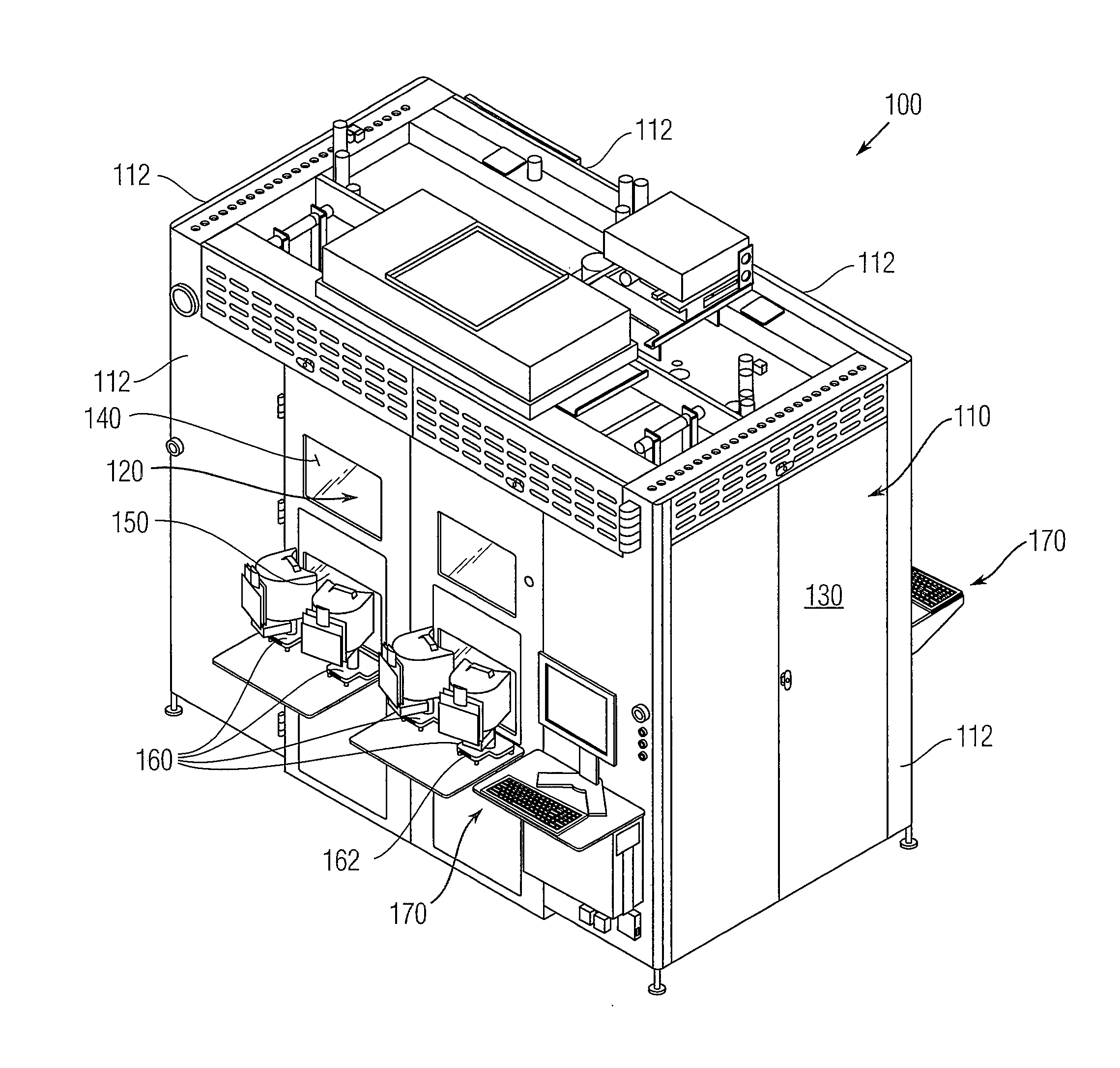
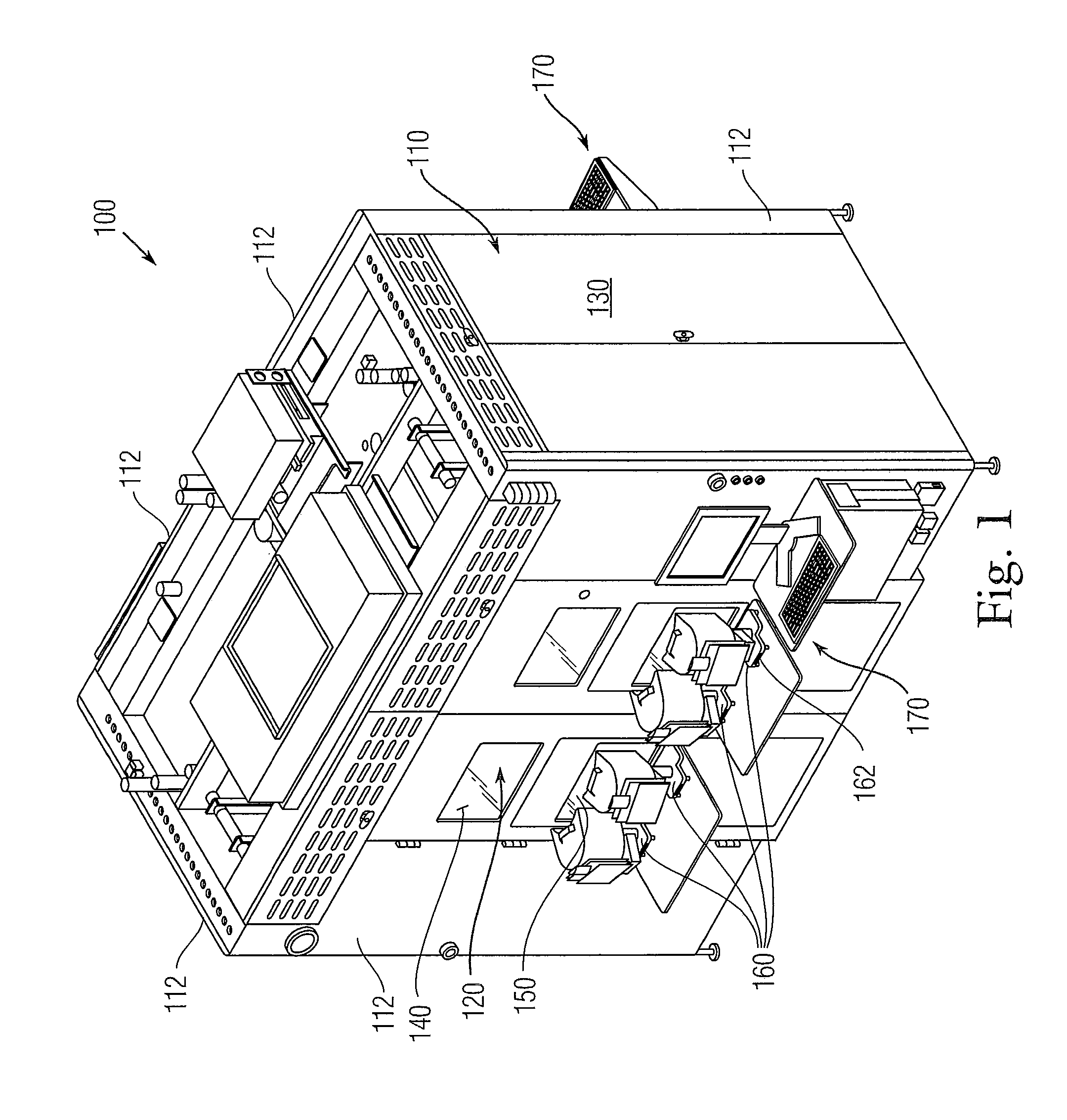
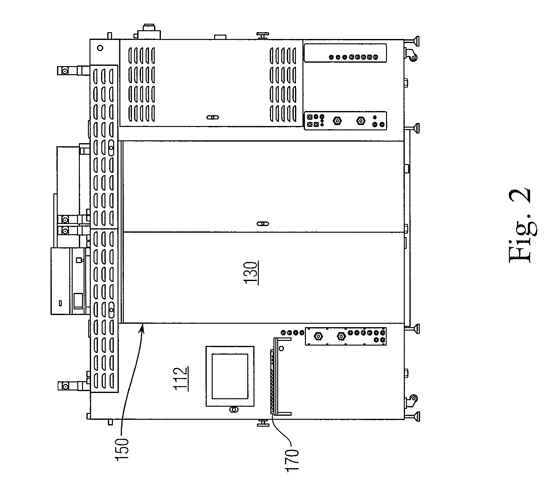
[0040]FIGS. 1-5 illustrate a system 100 for performing a wet etching process in accordance with one embodiment of the present invention. The system 100 can thus be thought of as being a wet-etching facility for manufacturing semiconductor devices.

[0041]In a wafer wet treatment process of a semiconductor device manufacturing process, there are generally an etching process and a cleaning process as mentioned hereinbefore. A single wafer wet treatment apparatus used in an etching process dispenses chemical etchant in a controlled manner on a substrate for inducing a chemical reaction during a fixed time. It will be understood that the terms “wafer” and “substrate” are used interchangeably herein. A single wafer wet treatment apparatus used in a cleaning process causes a chemical solution to be dispensed onto a substrate and can also include a scrubbing device to mechanically scrub the substrate. Each of the wet treatment apparatuses can include a bath that collects fluids that overflow...


PUM

PropertyMeasurementUnit
Thicknessaaaaaaaaaa
Depthaaaaaaaaaa
Heightaaaaaaaaaa

Abstract

A system and method for performing a wet etching process is disclosed. The system includes multiple processing stations accessible by a transfer device, including a measuring station to optically measure the thickness of a substrate, a controller to calculate an etch recipe for the substrate, in real time, and cause a single wafer wet etching station to etch the substrate according to the recipe. In addition, the system can measure the after etch thickness and calculate etch recipes, in real time, as a function of the final measurements of a previous substrate. The system can also include an in situ end point detection device for detecting the TSV reveal point while etching TSVs substrates. The system provides an automated solution to adjust etch recipe parameters in real time according to feedback concerning previously etched wafers and precisely control the TSV reveal height and etch duration using end point detection.

Description

TECHNICAL FIELD[0001]The present invention generally relates to a system and method for etching semiconductor wafers for integrated circuits and, more specifically, relates to a system and method for etching semiconductor wafers (integrated circuit substrates) using a wet etching process that results in the etching of the wafer to a precise and uniform thickness.BACKGROUND[0002]2.5 and 3D Integration is becoming a reality in device manufacturing. A critical process step is the thinning of the silicon wafer to reveal the metal filled Through Silicon Via (TSV). Grinding is used to remove the bulk of the silicon wafer. Currently a multistep sequence of processes that includes chemical mechanical planarization (CMP) and plasma etching has been used to complete the final thinning of the silicon. However, this conventional process has a number of disadvantages associated therewith including but not limited to the complexity of the process and the associated costs. As described hereinafter...

Claims


Application Information

Patent Timeline
IPC IPC(8): H01L21/66H01L21/67G01N21/55G06F17/50
CPCH01L22/12G01N21/55G06F17/50H01L21/67075H01L21/67046H01L21/67051H01L21/6708H01L21/67253H01L2924/0002H01L22/26H01L2924/00G06F30/00
Inventor MAUER, LAURALAWRENCE, ELENATADDEI, JOHNYOUSSEF, RAMEY
Owner VEECO INSTR
Learn More