Magnetic electronic device and manufacturing method thereof

a technology of electromagnetic electronic devices and manufacturing methods, applied in semiconductor devices, digital storage, instruments, etc., can solve the problems of large power consumption, large unwanted heat generation, and small generated signal, and achieve the effect of enhancing thermal stability and high reactivity

Active Publication Date: 2014-09-11
NATIONAL TSING HUA UNIVERSITY
View PDF2 Cites 12 Cited by
  • Summary
  • Abstract
  • Description
  • Claims
  • Application Information

AI Technical Summary

Benefits of technology

[0019]As mentioned above, in the magnetic electronic device and manufacturing method thereof according to this invention, a capping layer is formed above the first metal oxidation layer and covers the first metal oxidation layer. Thereby, the capping layer of high reactivity can absorb the extra diffusing oxygen and boron atoms so that the magnetization and perpendicular anisotropy of the bilayer structure of CoFeB layer / oxide layer can be increased and the thermal stability of the CoFeB layer (magnetic layer) can be enhanced.

Problems solved by technology

Both SRAM and DRAM are volatile since they need external periodic current supply all the time to retain the stored data, and therefore lots of unwanted heat would be generated and the power consumption is relatively large.
In early days, MRAM cell is made by the effect of anisotropic magnetoresistance (AMR) to create different resistance levels, but the generated signal is too small to meet the practical requirements.
After the as-grown amorphous CoFeB experiences an annealing treatment, a good texturing (001) can be generated at the interface of CoFeB and MgO, and such texturing results in considerable magnetoresistance.
In all related literatures of CoFeB with perpendicular anisotropy, the unit-volume saturation magnetization of CoFeB has only reached 1000 emu / c.c., and the magnetic anisotropy energy thereof is still insufficient.
In practical MRAM manufacturing process, manufacturing a MTJ (magnetic tunnel junction) itself is a big challenge, but other problems will also be encountered in the integration of the front-end and back-end processes.
The most important problem in those processes is the thermal budget of MTJs.

Method used


Image

  • Magnetic electronic device and manufacturing method thereof
  • Magnetic electronic device and manufacturing method thereof
  • Magnetic electronic device and manufacturing method thereof

Examples


Embodiment Construction

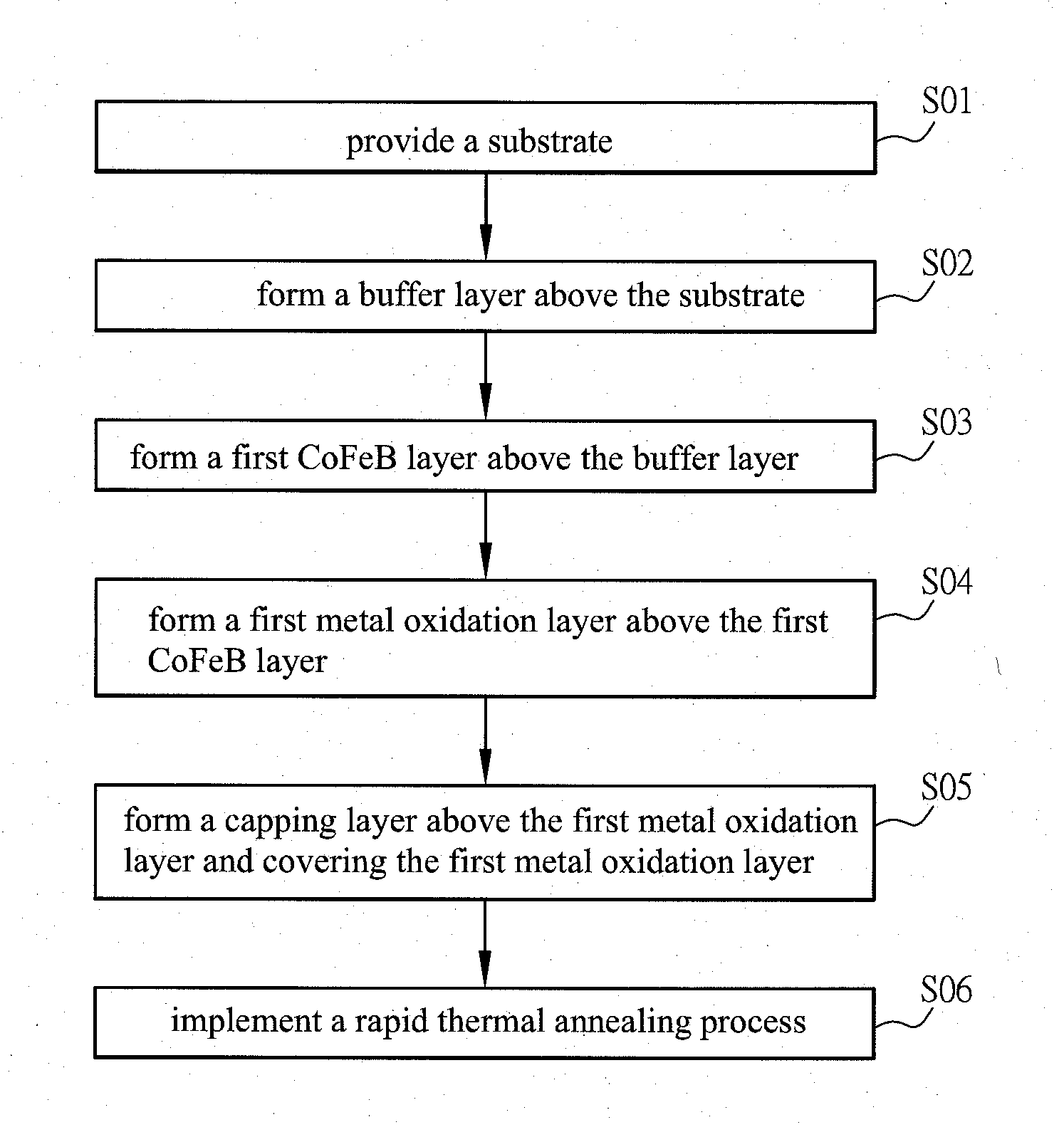
[0030]The present invention will be apparent from the following detailed description, which proceeds with reference to the accompanying drawings, wherein the same references relate to the same elements.

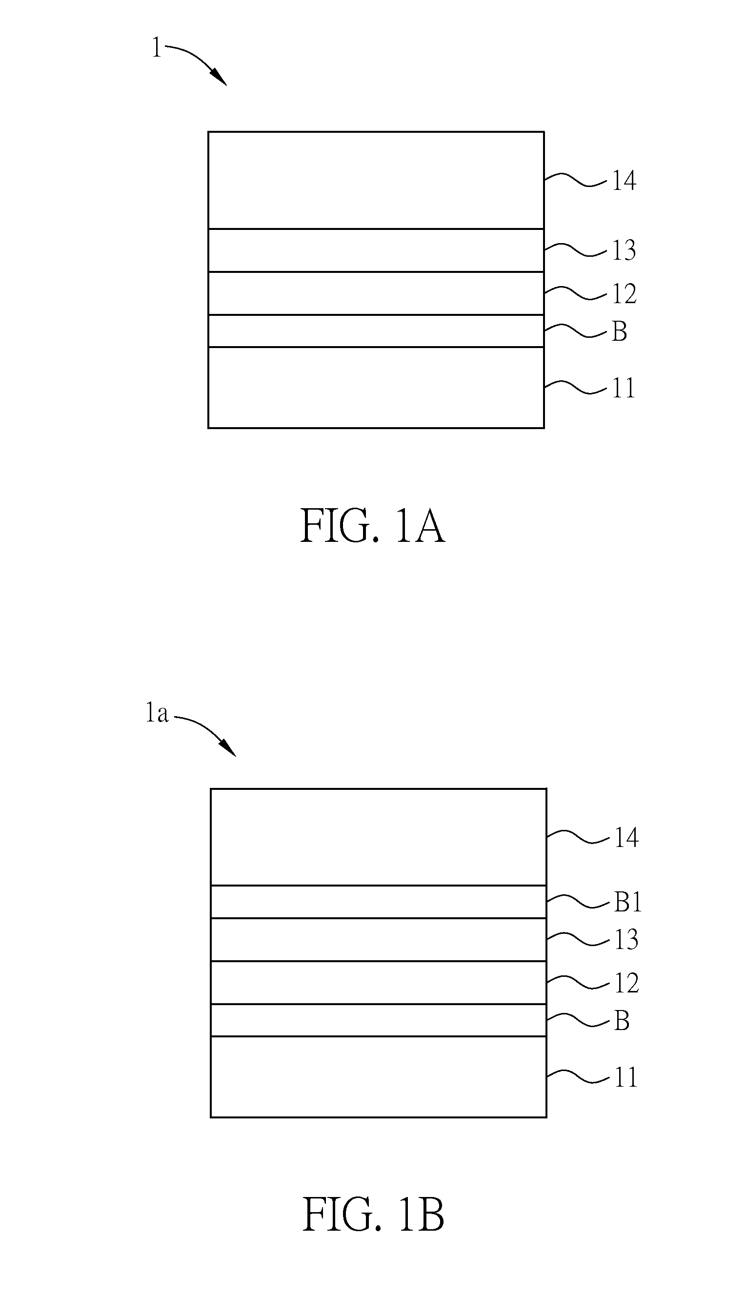
[0031]FIG. 1A is a schematic diagram of a magnetic electronic device 1 according to a preferred embodiment of this invention.

[0032]As shown in FIG. 1A, the magnetic electronic device 1 includes a substrate 11, a buffer layer B, a first CoFeB layer 12, a first metal oxidation layer 13 and a capping layer 14. Herein, the magnetic electronic device 1 can be applied to a memory or a magnetic field sensor. The said memory is magnetic random access memory (MRAM) or racetrack memory for example, and the said magnetic field sensor can be used in a geomagnetic sensing circuit for example.

[0033]The material of the substrate 11 can include silicon or silica, and herein SiO2 is used as the substrate 11. Otherwise, the substrate 11 can be glass. The first CoFeB layer 12 is disposed above the subst...


PUM

PropertyMeasurementUnit
thicknessaaaaaaaaaa
thicknessaaaaaaaaaa
temperatureaaaaaaaaaa

Abstract

A magnetic electronic device comprises a substrate, a buffer layer, a first CoFeB layer, a first metal oxidation layer and a capping layer. The buffer layer is disposed above the substrate. The first CoFeB layer is disposed above the buffer layer. The first metal oxidation layer is disposed above the first CoFeB layer. The capping layer is disposed above the first metal oxidation layer and covers the first metal oxidation layer. A manufacturing method of the magnetic electronic device is also disclosed.

Description

CROSS REFERENCE TO RELATED APPLICATIONS[0001]This Non-provisional application claims priority under 35 U.S.C. §119(a) on Patent Application No(s). 102108136 filed in Taiwan, Republic of China on Mar. 7, 2013, the entire contents of which are hereby incorporated by reference.BACKGROUND OF THE INVENTION[0002]1. Field of Invention[0003]The invention relates to a magnetic electronic device and a manufacturing method thereof and, in particular, to a magnetic electronic device and a manufacturing method thereof wherein the magnetic property of the free layer is adjusted.[0004]2. Related Art[0005]The concept of magnetic random access memory (MRAM) was brought up by Andreas Neyc with his colleagues of the Paul Drude institute in Germany. In MRAM, ferromagnetic metal is used and the data bit is stored by different relative magnetization alignment of the recording layer (free layer) and the reference layer (pinned layer), where parallel and anti-parallel magnetization alignment can result in ...

Claims


Application Information

Patent Timeline
Patent Type & Authority Applications(United States)
IPC IPC(8): H01L43/02H01L43/12
CPCH01L43/12H01L43/02G11C11/161H10N50/10H10N50/01H10N50/85H10N50/80
Inventor LAI, CHIH-HUANGWANG, DING-SHUO
Owner NATIONAL TSING HUA UNIVERSITY
Why Eureka
Try Eureka