Nonvolatile resistive memory element with an oxygen-gettering layer

a nonvolatile resistive memory element and oxygen-gettering technology, applied in information storage, static storage, digital storage, etc., can solve the problems of inability to reliably occur, inability to form, switch current, and forming voltage of traditional nonvolatile memory technology, and achieve more thermodynamically favorable oxygen gettering, the effect of increasing the thickness of the sio2 interfacial layer

Active Publication Date: 2014-09-18
INTERMOLECULAR
View PDF4 Cites 24 Cited by
  • Summary
  • Abstract
  • Description
  • Claims
  • Application Information

AI Technical Summary

Benefits of technology

[0009]Embodiments according to the invention set forth a ReRAM nonvolatile memory element that includes a novel oxygen-gettering layer and methods of forming the same. The oxygen-gettering layer is formed as part of an electrode stack, and its constituents are selected to be more thermodynamically favorable in gettering oxygen than other layers of the top electrode stack. In some embodiments, the Gibbs free energy of formation (ΔfG°) of an oxide of the oxygen-gettering layer is less (i.e., more negative) than the Gibbs free energy of formation of an oxide of the surrounding layers of the electrode stack. In such embodiments, the oxygen-gettering layer reacts with oxygen present in the surrounding layers of the electrode stack, thereby preventing this oxygen from diffusing into nearby silicon layers and increasing the thickness of an SiO2 interfacial layer. In some embodiments, the Gibbs free energy of formation of an oxide of the oxygen-gettering layer is less than the Gibbs free energy of formation of SiO2 in the interfacial layer of the nonvolatile memory element, so that the thickness of the interfacial layer can be reduced to a desired thickness with a thermal anneal process.

Problems solved by technology

However, as device dimensions shrink, scaling issues pose challenges for traditional nonvolatile memory technology.
If the silicon dioxide layer in a resistive switching device is too thick, the forming voltage, switching current, and switching voltage of the device are undesirably high.
If the silicon dioxide layer in the resistive switching device is too thin, bistable switching may not occur reliably.

Method used


Image

  • Nonvolatile resistive memory element with an oxygen-gettering layer
  • Nonvolatile resistive memory element with an oxygen-gettering layer
  • Nonvolatile resistive memory element with an oxygen-gettering layer

Examples


Embodiment Construction

[0021]Materials used as the switching layer of a nonvolatile resistive memory element are generally required to have bistable electrical switching properties and, ideally, can be operated with low switching current and formed with a minimal forming voltage. A nonvolatile memory element with a variable resistance layer and a novel oxygen-gettering layer, and methods of forming the same, are described. The novel variable resistance layer has bistable resistance properties and includes a high-K dielectric layer and a silicon dioxide (SiO2) interfacial layer. The novel oxygen-gettering layer includes an oxygen-gettering material that can prevent unwanted growth and / or reduce the thickness of the interfacial layer during fabrication of the memory element.

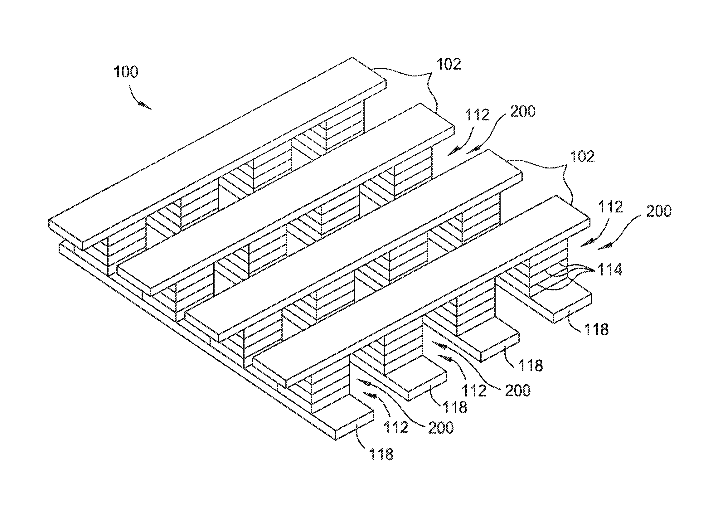
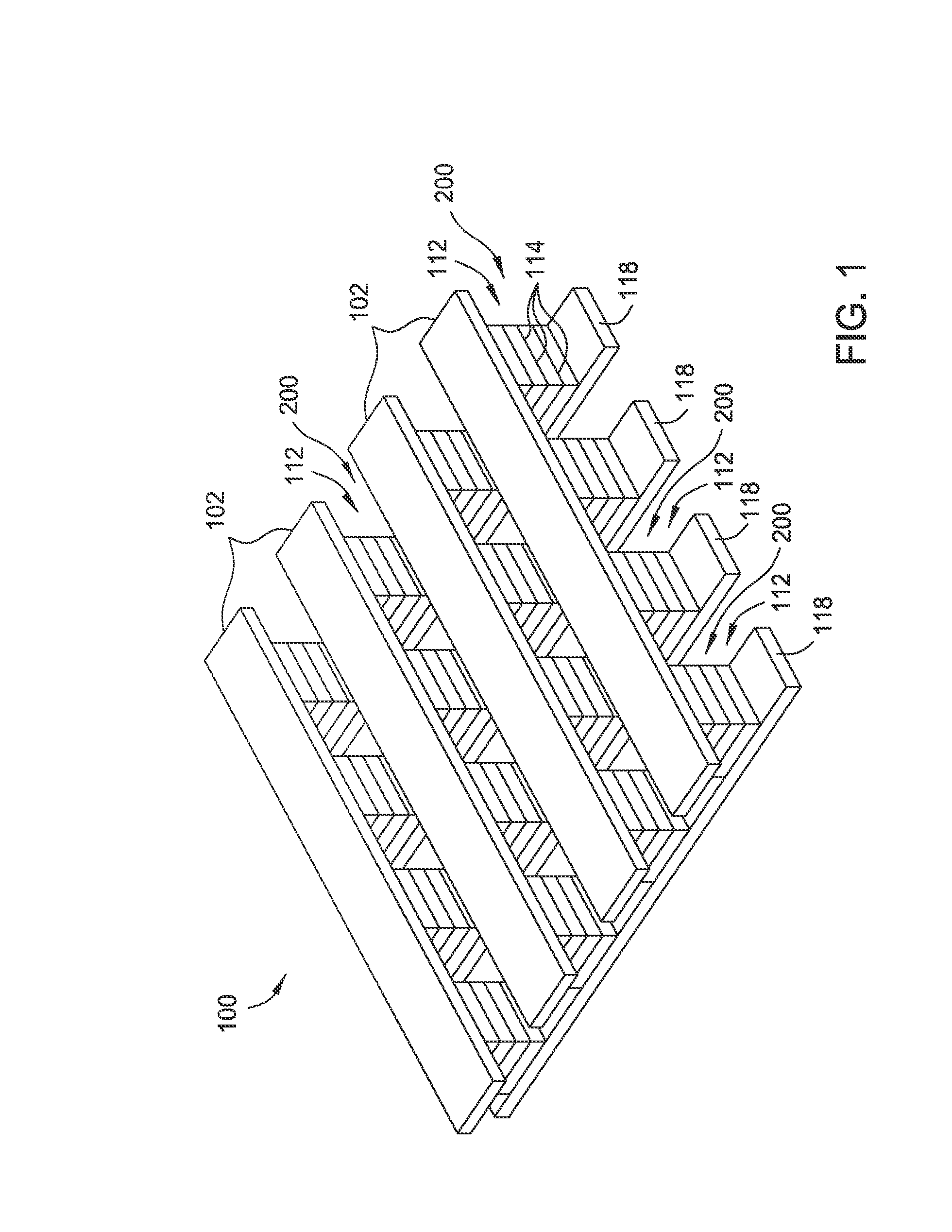
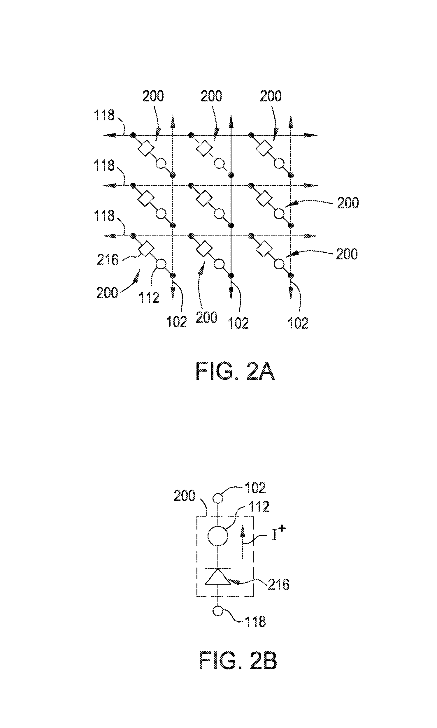
[0022]FIG. 1 is a perspective view of a memory array 100 of memory (elements) devices 200. Memory array 100 may be part of a larger memory device or other integrated circuit structure, such as a system-on-a-chip type device. Memory array...


PUM


Abstract

A nonvolatile resistive memory element includes an oxygen-gettering layer. The oxygen-gettering layer is formed as part of an electrode stack, and is more thermodynamically favorable in gettering oxygen than other layers of the electrode stack. The Gibbs free energy of formation (ΔfG°) of an oxide of the oxygen-gettering layer is less (i.e., more negative) than the Gibbs free energy of formation of an oxide of the adjacent layers of the electrode stack. The oxygen-gettering layer reacts with oxygen present in the adjacent layers of the electrode stack, thereby preventing this oxygen from diffusing into nearby silicon layers to undesirably increase an SiO2 interfacial layer thickness in the memory element and may alternately be selected to decrease such thickness during subsequent processing.

Description

BACKGROUND[0001]1. Field of the Invention[0002]This invention relates to nonvolatile resistive memory elements, and more particularly, to a nonvolatile resistive memory element with an oxygen-gettering layer.[0003]2. Description of the Related Art[0004]Nonvolatile memory elements are used in devices requiring persistent data storage, such as digital cameras and digital music players, as well as in computer systems. Electrically-erasable programmable read only memory (EPROM) and NAND flash are nonvolatile memory technologies currently in use. However, as device dimensions shrink, scaling issues pose challenges for traditional nonvolatile memory technology. This has led to the investigation of alternative nonvolatile memory technologies, including resistive switching nonvolatile memory.[0005]Resistive-switching-based nonvolatile memory is formed using memory elements that are bistable, i.e., having two stable states with different resistances. A bistable memory element can be placed i...

Claims


Application Information

Patent Timeline
Patent Type & Authority Applications(United States)
IPC IPC(8): G11C13/00
CPCG11C13/0002G11C13/0007G11C2213/15G11C2213/33G11C2213/34G11C2213/52H10B63/20H10B63/80H10N70/801H10N70/24H10N70/883H10N70/826H10N70/8833H10N70/841H10N70/881
Inventor CHIANG, TONY P.PRAMANIK, DIPANKARWELING, MILIND
Owner INTERMOLECULAR
Why Eureka
Try Eureka