
Eureka
For R&D, Eureka makes reading and utilizing patents & technical documents easy.
Eureka AIR
Designed for self-driven R&D workflows. Generate viable solutions, solve complex R&D challenges, empower your innovation with AI.

Eureka Materials
Designed for material experts only. Revolutionize your material R&D, from search, analyze, to developing new materials.

TechResearch
Generate reliable direction feasibility study reports for your R&D in just a few steps.

TechSeek
Discover and master advanced knowledge NOW. Basics, ideas, possibilities, all at once.

TechMind
As an expert in R&D Theories, TechMind can generates customized viable solutions instantly.

TechRisk
Analyze your overall solution with one click, know your potential R&D risks in advance.

TechMonitor
Get weekly tech updates, stay abreast of the latest tech innovations and key insights.
Method for manufacturing graphene film and graphene channel of transistor
- Summary
- Abstract
- Description
- Claims
- Application Information
AI Technical Summary
Benefits of technology
Problems solved by technology
Method used
Image

Examples
example 2
Analysis of Graphene Film
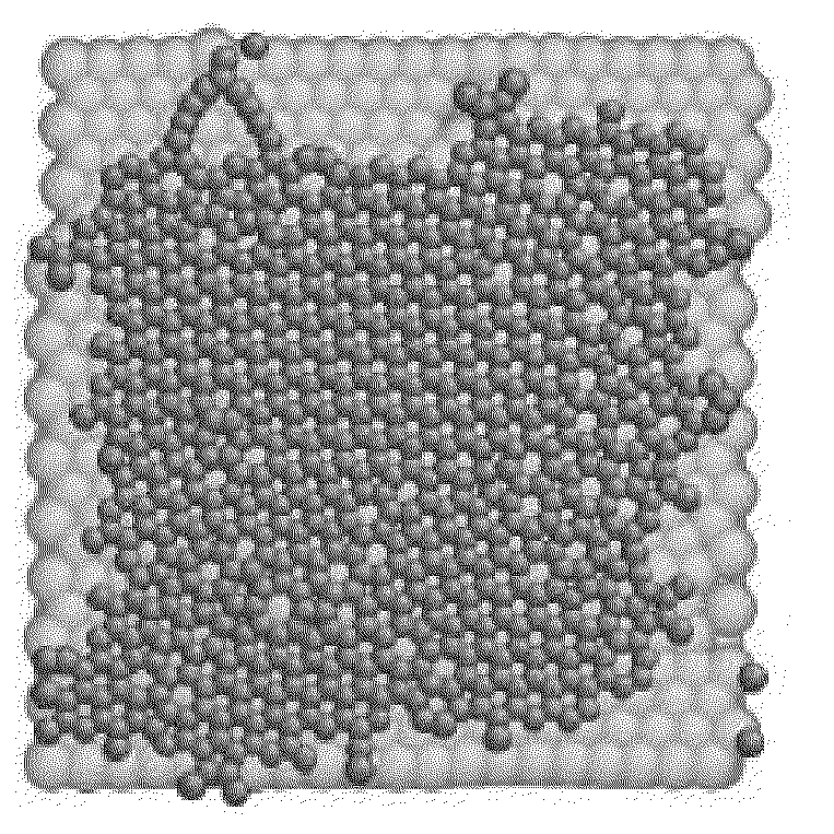
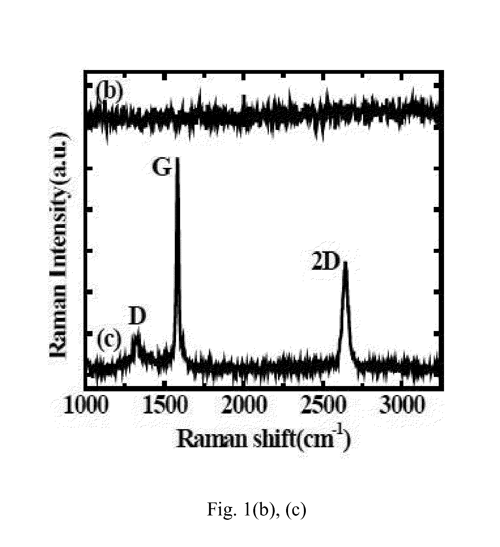
[0049]The scanning tunneling microscope (STM) images of the graphene film in the present invention were taken by using RHK-SPM 100 system under ambient circumstance. The Raman measurements were performed by using HORIBA Jobin Yvon HR800UV spectrum system on the films transferred to the SiO2 / Si substrates.
[0050]The 4.2×4.2 nm2 STM image of the graphene film grown on a Cu foil at 300° C. measured under a tunneling current of 1.05 nA and a bias of 1.6 V was shown in FIG. 1(a). As shown in the figure, completely hexagonal structure of carbon atoms can be observed. These results suggested that by using the atomic carbon source, graphitization could take place at a low temperature of 300° C. To verify if the graphene film was formed after high-temperature furnace annealing step or after MBE growth step, the Raman spectrum of the Cu foil measured after high-temperature furnace annealing was shown in FIG. 1(b). No characteristic peaks for graphene were observed in t...
example 3
Analysis of Graphene Film Fabricated into Back-Gate Transistor
[0051]The graphene film transferred onto the 600 nm SiO2 / p-type Si substrate was fabricated into a back-gate transistor. As shown in FIG. 2(a), this is an image analysis diagram of the transistor device analyzed by the scanning electron microscope (SEM). The graphene stripes were defined by using the standard photolithography procedure with O2 plasma etching. After Au metal evaporation for source / drain terminals, a graphene transistor having a channel with 10 μm channel width and 50 μm channel length was fabricated. In addition, the drain currents of the back-gate transistor measured under different gate biases were shown in FIG. 2(b). As shown in the figure, a significant current modulation was observed for the device. By fitting the curve using the equation μ=(dID / dVg) / (∈VDW / ToxL), where Tox, W and L represent the gate dielectric thickness, channel width and channel length, respectively. ∈ is a dielectric constant of di...
PUM
 Abstract
Description
Claims
Application Information
 - R&D Engineer
- R&D Manager
- IP Professional
- Industry Leading Data Capabilities
- Powerful AI technology
- Patent DNA Extraction
Browse by: Latest US Patents, China's latest patents, Technical Efficacy Thesaurus, Application Domain, Technology Topic, Popular Technical Reports.
© 2024 PatSnap. All rights reserved.Legal|Privacy policy|Modern Slavery Act Transparency Statement|Sitemap|About US| Contact US: help@patsnap.com