Semiconductor structure and process thereof

Active Publication Date: 2014-09-25
UNITED MICROELECTRONICS CORP
View PDF6 Cites 25 Cited by
  • Summary
  • Abstract
  • Description
  • Claims
  • Application Information

AI Technical Summary

Benefits of technology

[0010]According to the above, the present invention provides a semiconductor structure and a process thereof, which integrates a capacitor process and a MOS transistor process to form transistors and capacitors by the same process, thereby simplifying processing steps and reducing processing costs. More specifically, a lower electrode of a capacitor is formed together with a

Problems solved by technology

As the integration of an integrated circuit increases and sizes of its semiconductor components shrink, it becomes a great issue to integrate these components

Method used


Image

  • Semiconductor structure and process thereof
  • Semiconductor structure and process thereof
  • Semiconductor structure and process thereof

Examples


Embodiment Construction

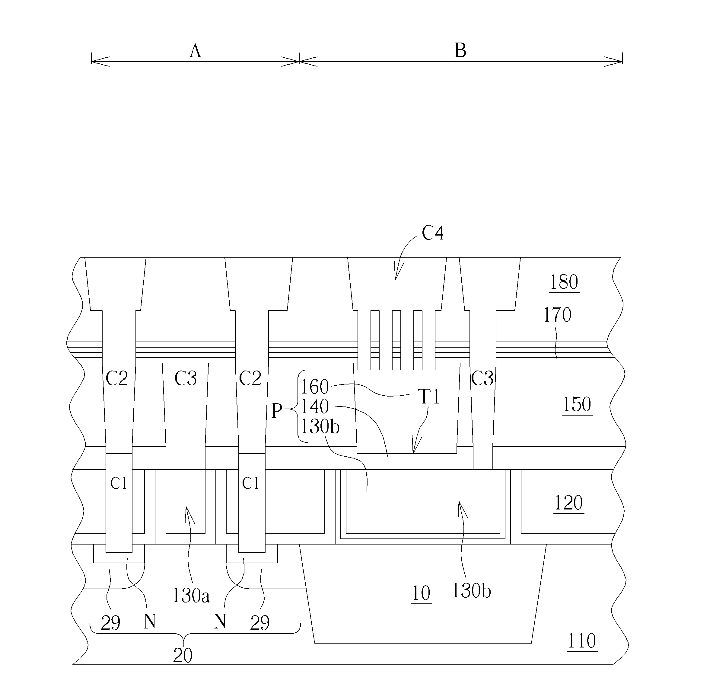
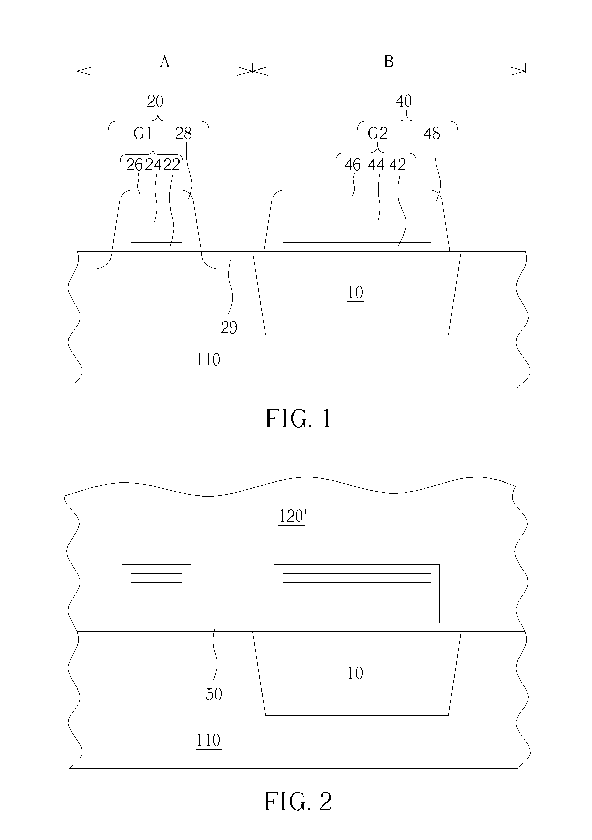
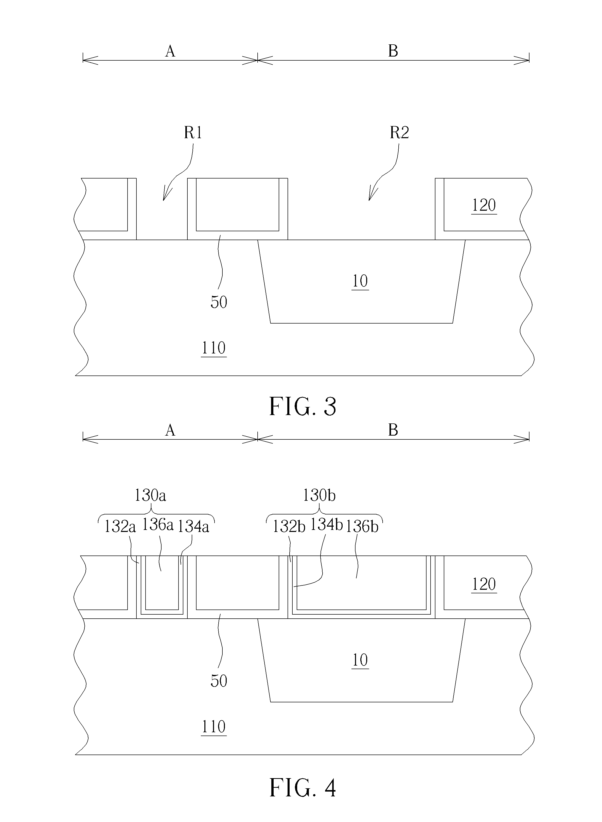
[0014]FIGS. 1-9 schematically depict cross-sectional views of a semiconductor process according to an embodiment of the present invention. As shown in FIG. 1, a substrate 110 is provided, wherein the substrate 110 has a first area A and a second area B. In this embodiment, the first area A is a transistor area for forming a MOS transistor therein, and the second area B is a capacitor area for forming a capacitor therein. In this embodiment, only one MOS transistor is depicted in the first area A, and one capacitor is depicted in the second are B to clarify and simplify the present invention, but the number of the MOS transistor or the capacitor is not restricted to one, it may be more than one, depending upon the needs. The substrate 110 may be a semiconductor substrate such as a silicon substrate, a silicon containing substrate, a III-V group-on-silicon (such as GaN-on-silicon) substrate, a graphene-on-silicon substrate or a silicon-on-insulator (SOI) substrate.

[0015]An isolation s...


PUM


Abstract

A semiconductor structure includes a metal gate, a second dielectric layer and a contact plug. The metal gate is located on a substrate and in a first dielectric layer, wherein the metal gate includes a work function metal layer having a U-shaped cross- sectional profile and a low resistivity material located on the work function metal layer. The second dielectric layer is located on the metal gate and the first dielectric layer. The contact plug is located on the second dielectric layer and in a third dielectric layer, thereby a capacitor is formed. Moreover, the present invention also provides a semiconductor process forming said semiconductor structure.

Description

BACKGROUND OF THE INVENTION[0001]1. Field of the Invention[0002]The present invention relates generally to a semiconductor structure and a process thereof, and more specifically to a semiconductor structure and a process thereof that integrates capacitors and transistors.[0003]2. Description of the Prior Art[0004]Each capacitor in a semiconductor component usually includes two electrodes and a dielectric layer between the two electrodes. This structure has been widely used in many semiconductor components such as dynamic random access memories (DRAM). A capacitor process often includes the following steps: a conductive layer is formed on a substrate and is patterned to forma lower electrode of the capacitor; a dielectric layer is formed on the lower electrode; then, another conductive layer covers the dielectric layer to form the capacitor.[0005]The materials of the electrodes may include polysilicon, polycide and metal. Thus, there are three fabricating methods for forming three ki...

Claims


Application Information

Patent Timeline
IPC IPC(8): H01L49/02H01L21/28H01L27/06
CPCH01L28/90H01L27/0629H01L21/28H01L28/60H01L29/4966H01L29/51H01L29/66545H01L28/75H01L29/40114H10B12/03H01L21/76802H01L21/76877H01L29/66477
Inventor HUNG, CHING-WENHUANG, CHIH-SENTSAO, PO-CHAO
Owner UNITED MICROELECTRONICS CORP
Why Eureka
Try Eureka