Method for manufacturing self-aligned thin film transistor

Active Publication Date: 2014-01-09
PEKING UNIV SHENZHEN GRADUATE SCHOOL
View PDF3 Cites 30 Cited by
  • Summary
  • Abstract
  • Description
  • Claims
  • Application Information

AI Technical Summary

Benefits of technology

[0018]Moreover, since the photoresist is exposed from a back surface of the substrate when the active region is processed, the gate electrode functions as a natural mask plate. In this way, it is unnecessary to fabricate a mask plate, reducing the cost and simplifying the processing steps. On the other hand, since the gate electrode functions as a mask plate, the channel region can be preciously aligned with the gate electrode, reducing the possibility of generating parasitic elements and improving the uniformity of the perform

Problems solved by technology

However, since the amorphous silicon thin film transistors have low mobility and easy performance degradation, the applications in the pixel driving of an OLED and in the integration of peripheral driving circuits of a LCD and OLED are limited.
Moreover, manufacturing the polycrystalline silicon thin film transistors needs a high temperature, the manufacturing cost is high, and the performance uniformity of the polycrystalline silicon thin film transistors is poor.
Thus, the polycrystalline silicon thin film transistors are not suitable to the large-size panel displays.
However, there is a disadvantage in the method for manufacturing the zinc oxide based thin film transistors.
Specifically, the resulting zinc oxide based thin film transistors have non-self-aligned structures, resulting in large parasitic elements existing in the transistors and uncontrollable characteristics discreteness.
The parasitic capa

Method used


Image

  • Method for manufacturing self-aligned thin film transistor
  • Method for manufacturing self-aligned thin film transistor
  • Method for manufacturing self-aligned thin film transistor

Examples


embodiment 1

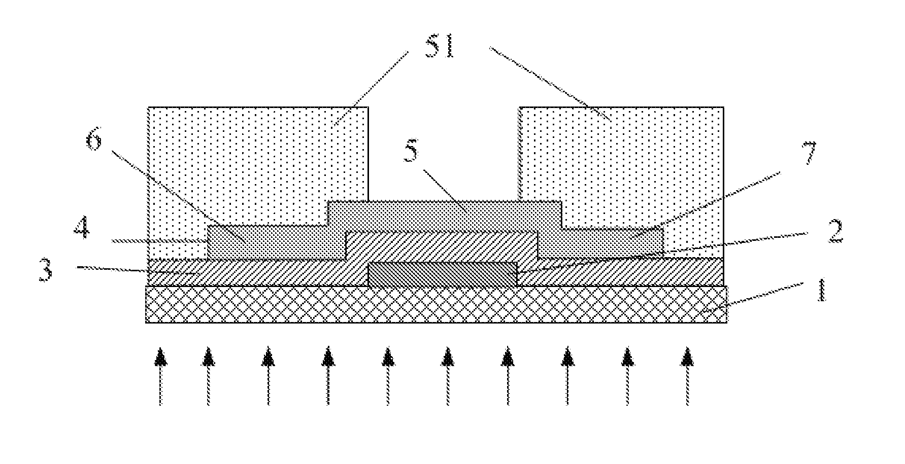
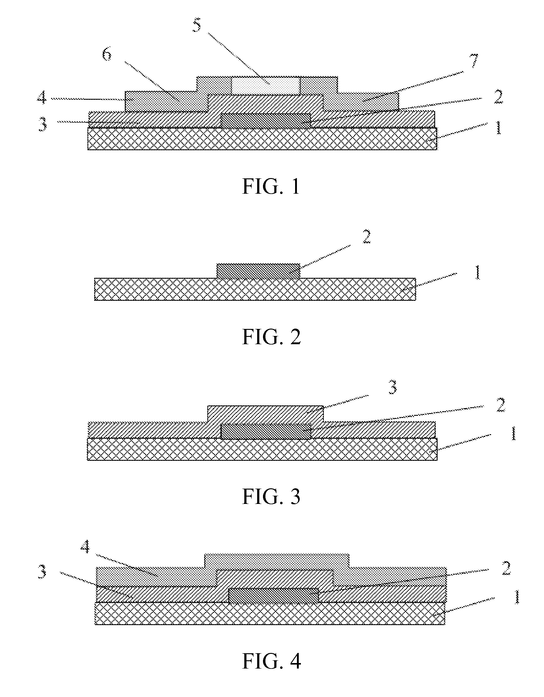
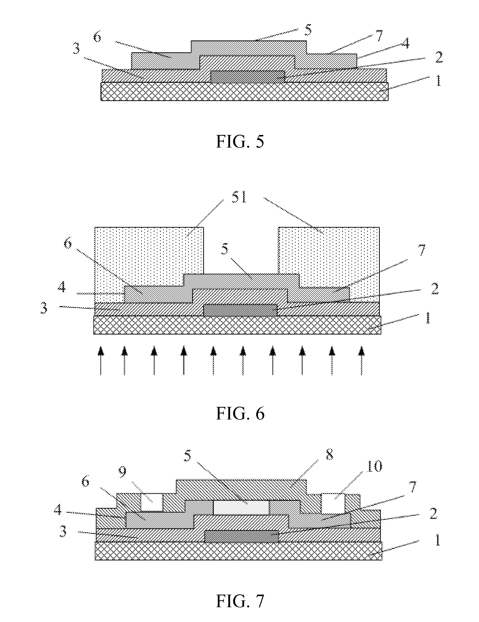
[0064]A method for manufacturing the thin film transistor according to the present embodiment is shown in FIGS. 2-8 and comprises the following steps.

[0065]11) As shown in FIG. 2, a metal film having a thickness of 100-300 nm is formed on a surface (such as a front surface) of the substrate 1. The metal film may be formed by magnetron sputtering and may be formed from chromium, molybdenum, titanium, aluminium or the like. Then, the metal film is processed accordingly so that the gate electrode 2 is formed. For example, the gate electrode 2 may be formed by performing lithographic and etching processes on the metal film. In the present example, the substrate 1 may be resistant to high temperature, such as a glass substrate, or may be not resistant to high temperature, such as a plastic substrate. For ease of description, the surface of the substrate on which the thin film transistor is manufactured is called a front surface.

[0066]12) As shown in FIG. 3, an insulating film having a th...

embodiment 2

[0075]Since the channel region 5 is oxidized by the oxygen plasma at a low temperature in the present invention, it is unnecessary to form a dielectric protection layer, simplifying the manufacturing process of transistors. However, the oxygen plasma has some effect on the protective photoresist layer. Although the advantage of using the photoresist layer as a protection layer lies in that the manufacturing process is simple, a portion of the photoresist may be destroyed by the oxygen plasma during the process, and thus the source and drain regions cannot be entirely protected from oxidation. Accordingly, for precisely protecting the source and drain regions, a dielectric protection layer may be formed and the formed dielectric protection layer can be subjected to high temperatures for the subsequent manufacturing process. The manufacturing steps are as follows.

[0076]21) As shown in FIG. 9, a metal film having a thickness of 100-300 nm is formed on the front surface of the substrate...

embodiment 3

[0084]In order to manufacture a transistor having a self-aligned structure, in the step 25) of the embodiment 2, a layer of positive photoresist may be coated and subjected to exposure, developing, etc. The detailed processes are as follows.

[0085]31) As shown in FIG. 17, a metal film having a thickness of 100-300 nm is formed on the front surface of the substrate 1. The metal film may be formed by magnetron sputtering and may be formed from chromium, molybdenum, titanium, aluminium or the like. Then, the metal film is processed accordingly, for example, subjected to photolithography and etching, so that the gate electrode 2 is formed. In the present embodiment, the substrate 1 may be resistant to a high temperature, such as a glass substrate, or may be not resistant to a high temperature, such as a plastic substrate.

[0086]32) As shown in FIG. 18, an insulting film having a thickness of 100-400 nm is formed on the front surface of the substrate 1. The insulting film may be formed fro...


PUM


Abstract

Disclosed is a method for manufacturing a self-aligned metal oxide thin film transistor. According to the present invention, a metal oxide semiconductor layer having a high carrier concentration is formed, and then a channel region which is self-aligned with a gate electrode is oxidized by a plasma having oxidbillity so that the channel region has a low carrier concentration and the source and drain regions have high carrier concentrations while the resulting transistor has a self-aligned structure. In addition, the threshold voltage of the transistor is controlled by the conditions under which the channel region of the transistor is subsequently oxidized by plasma having oxidbillity at a low temperature. Therefore, the controllability of the characteristics of the transistor is improved significantly, and the manufacturing process is simplified.

Description

FIELD OF THE INVENTION[0001]The present invention relates to a method for manufacturing a thin film transistor, especially to a method for manufacturing a self-aligned metal oxide semiconductor thin film transistor.BACKGROUND OF THE INVENTION[0002]Thin film transistors are used as switching elements or integrated elements of peripheral driving circuits in various display devices. Presently, the widely used thin film transistors mainly include amorphous silicon thin film transistors and polycrystalline silicon thin film transistors. However, since the amorphous silicon thin film transistors have low mobility and easy performance degradation, the applications in the pixel driving of an OLED and in the integration of peripheral driving circuits of a LCD and OLED are limited. Moreover, manufacturing the polycrystalline silicon thin film transistors needs a high temperature, the manufacturing cost is high, and the performance uniformity of the polycrystalline silicon thin film transistor...

Claims


Application Information

Patent Timeline
IPC IPC(8): H01L29/66
CPCH01L29/66742H01L29/4908H01L29/78618H01L29/7869H01L29/78696H01L29/66969
Inventor ZHANG, SHENGDONGHE, XINWANG, YIHAN, DEDONGHAN, RUQI
Owner PEKING UNIV SHENZHEN GRADUATE SCHOOL
Why Eureka
Try Eureka