Semiconductor device and manufacturing method thereof

a semiconductor and manufacturing method technology, applied in the direction of semiconductor/solid-state device manufacturing, semiconductor devices, electrical devices, etc., can solve the problems of poor electrical characteristics of transistors, difficult processing, and reduced resistance of semiconductor films, so as to reduce the concentration of impurities in semiconductor films, reduce the defect of oxide semiconductor films, and reduce the effect of oxide semiconductor films

Active Publication Date: 2014-10-02
SEMICON ENERGY LAB CO LTD
View PDF9 Cites 16 Cited by
  • Summary
  • Abstract
  • Description
  • Claims
  • Application Information

AI Technical Summary

Benefits of technology

[0016]Consequently, diffusion of an impurity which is a constituent element of wirings and electrodes, such as copper, aluminum, gold, silver, or molybdenum, into the semiconductor film can be suppressed. In addition, the concentration of the impurity in the semiconductor film can be decreased.
[0017]In one embodiment of the present invention, in a semiconductor device including an oxide semiconductor film, defects in the oxide semiconductor film can be reduced. Further, in one...

Problems solved by technology

However, there are problems in that copper, aluminum, gold, silver, molybdenum, or the like, which is a constituent element of the wiring, is difficult to process, and they are diffused in a semiconductor film in the course of the processing.
Copper, aluminum, gold, silver, molybdenum, or the like, which is a constituent element of the wiring, is one of ...

Method used


Image

  • Semiconductor device and manufacturing method thereof
  • Semiconductor device and manufacturing method thereof
  • Semiconductor device and manufacturing method thereof

Examples


embodiment 1

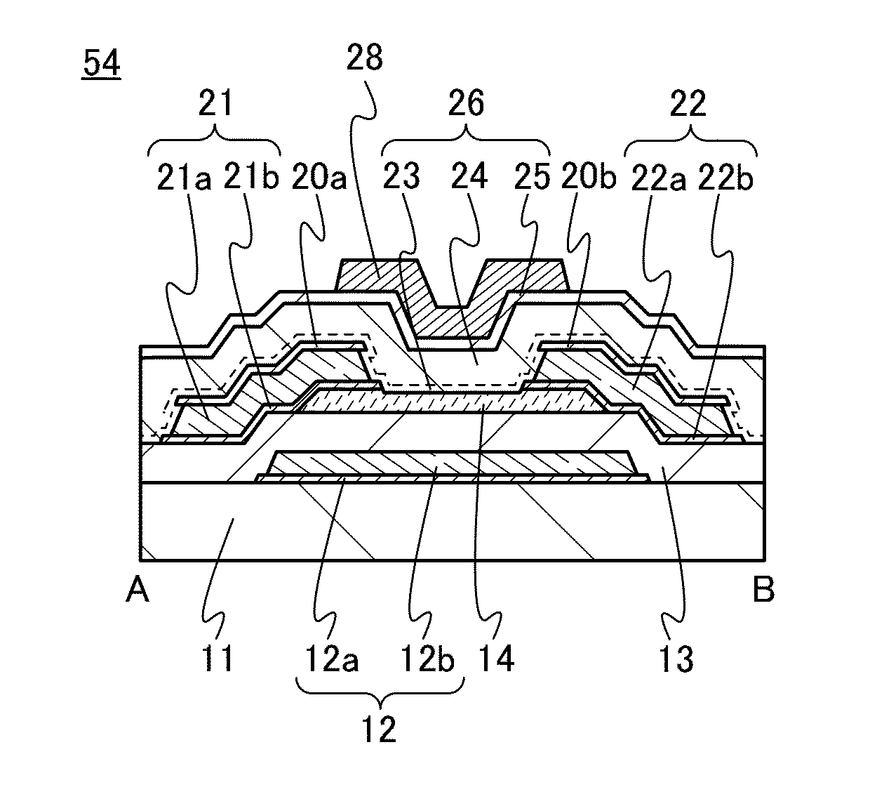
[0039]In this embodiment, a semiconductor device which is one embodiment of the present invention and a manufacturing method thereof are described with reference to drawings.

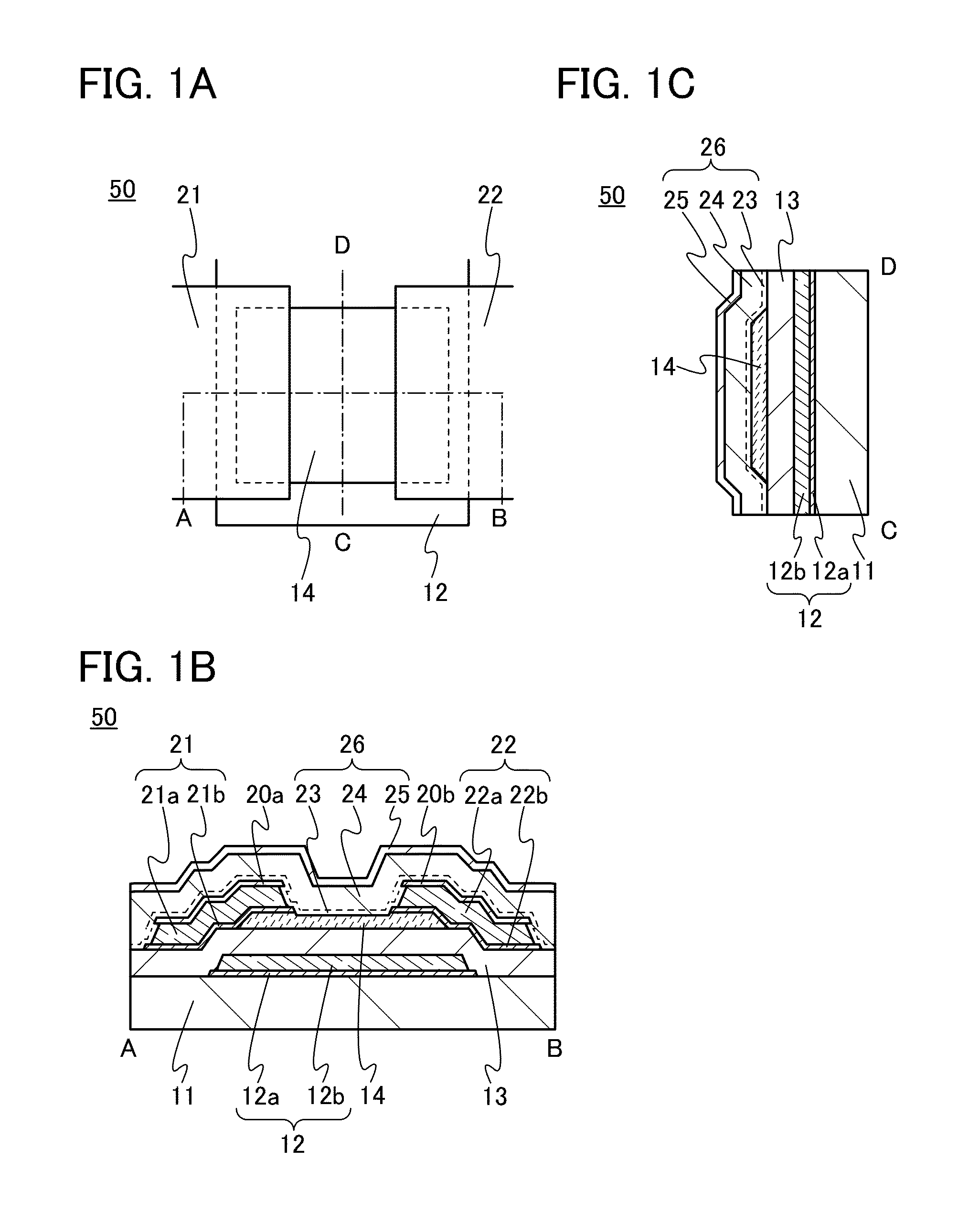
[0040]FIGS. 1A to 1C are a top view and cross-sectional views of a transistor 50 of a semiconductor device. The transistor 50 shown in FIGS. 1A to 1C is a channel-etched transistor. FIG. 1A is a top view of the transistor 50, FIG. 1B is a cross-sectional view taken along dashed-dotted line A-B in FIG. 1A, and FIG. 1C is a cross-sectional view taken along dashed-dotted line C-D in FIG. 1A. Note that in FIG. 1A, a substrate 11, a gate insulating film 13, an oxide insulating film 23, an oxide insulating film 24, a nitride insulating film 25, and the like are not illustrated for clarity.

[0041]The transistor 50 illustrated in FIGS. 1B and 1C includes a gate electrode 12 provided over the substrate 11, the gate insulating film 13 formed over the substrate 11 and the gate electrode 12, a semiconductor film 14 overlappi...

embodiment 2

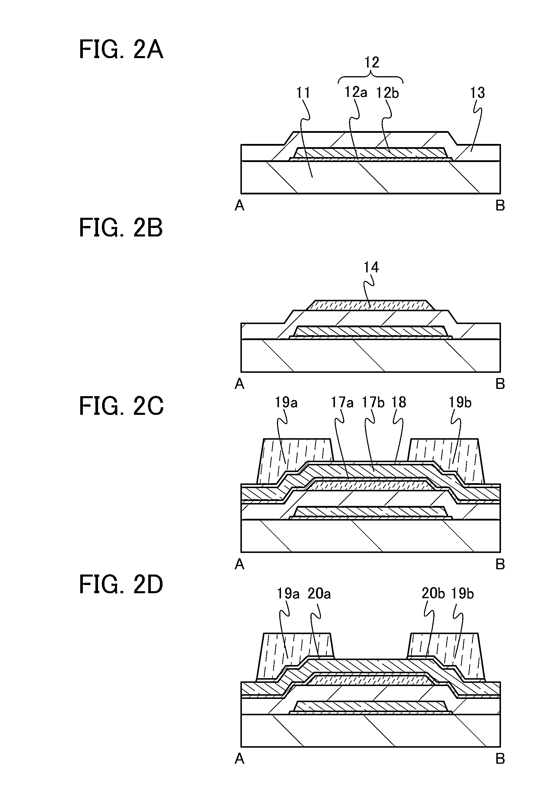
[0171]In this embodiment, a method for forming a pair of electrodes which is different from that in Embodiment 1 is described with reference to FIGS. 2A to 2D and FIGS. 4A to 4D.

[0172]In a manner similar to that in Embodiment 1, through the process of FIGS. 2A to 2D, the gate electrode 12, the gate insulating film 13, the semiconductor film 14, the film 17a to be the first protective films, the conductive film 17b, the masks 19a and 19b, and the pair of second protective films 20a and 20b are formed over the substrate 11 as illustrated in FIG. 2D.

[0173]Next, as illustrated in FIG. 4A, part of the conductive film 17b is etched using the masks 19a and 19b to form the pair of conductive films 21a and 22a. Here, in a manner similar to that in Embodiment 1, a method is employed in which the film 17a to be the first protective films is not etched and the conductive film 17b is selectively etched. Consequently, the semiconductor film 14 is not exposed in this etching step; thus, the metal ...

embodiment 3

[0188]In this embodiment, a semiconductor device having a transistor in which the amount of defects in an oxide semiconductor film can be further reduced when the oxide semiconductor film is used as a semiconductor film is described with reference to drawings. The transistor described in this embodiment is different from that in Embodiment 1 in that a multilayer film having an oxide semiconductor film and an oxide film in contact with the oxide semiconductor film is included.

[0189]FIGS. 5A to 5C are a top view and cross-sectional views of a transistor 60 included in the semiconductor device. FIG. 5A is a top view of the transistor 60, FIG. 5B is a cross-sectional view taken along dashed-dotted line A-B in FIG. 5A, and FIG. 5C is a cross-sectional view taken along dashed-dotted line C-D in FIG. 5A. Note that in FIG. 5A, the substrate 11, one or more of components of the transistor 60 (e.g., the gate insulating film 13), the oxide insulating film 23, the oxide insulating film 24, the ...


PUM


Abstract

The stability of steps of processing a wiring formed using copper or the like is increased. The concentration of impurities in a semiconductor film is reduced. Electrical characteristics of a semiconductor device are improved. A semiconductor device includes a semiconductor film, a pair of first protective films in contact with the semiconductor film, a pair of conductive films containing copper or the like in contact with the pair of first protective films, a pair of second protective films in contact with the pair of conductive films on the side opposite the pair of first protective films, a gate insulating film in contact with the semiconductor film, and a gate electrode overlapping with the semiconductor film with the gate insulating film therebetween. In a cross section, side surfaces of the pair of second protective films are located on the outer side of side surfaces of the pair of conductive films.

Description

BACKGROUND OF THE INVENTION[0001]1. Field of the Invention[0002]The present invention relates to a semiconductor device including a transistor and a method for manufacturing the semiconductor device.[0003]2. Description of the Related Art[0004]Transistors used for most flat panel displays typified by a liquid crystal display device or a light-emitting display device are formed using a silicon semiconductor such as amorphous silicon, single crystal silicon, or polycrystalline silicon provided over a glass substrate. Further, such a transistor employing the silicon semiconductor is used in integrated circuits (ICs) and the like.[0005]Further, in accordance with increasing size and increasing definition of a flat panel display, the driving frequency is increased and the resistance and the parasitic capacitance of a wiring are increased, so that wiring delay occurs. In order to inhibit the wiring delay, a technique for forming a wiring using copper has been studied (Patent Document 1).R...

Claims


Application Information

Patent Timeline
IPC IPC(8): H01L27/12
CPCH01L27/1214H01L27/1259H01L27/1225H01L29/7869H01L27/124H01L29/78618
Inventor YAMAZAKI, SHUNPEIJINTYOU, MASAMINAKAZAWA, YASUTAKASHIMA, YUKINORI
Owner SEMICON ENERGY LAB CO LTD
Why Eureka
Try Eureka