Charge pump circuit

Inactive Publication Date: 2014-10-16
OPTIS CIRCUIT TECH LLC
View PDF11 Cites 15 Cited by
  • Summary
  • Abstract
  • Description
  • Claims
  • Application Information

AI Technical Summary

Benefits of technology

[0009]To address these needs, a first aspect of the present invention relates to a more concise electrical structure. The inventors propose a new architecture for charge pump circuits enabling as much flexibility a

Problems solved by technology

Therefore, almost two thirds of the current is wasted by the charge pump circuit's inherent consumption.
Conversely, the charge pump ci

Method used


Image

  • Charge pump circuit
  • Charge pump circuit
  • Charge pump circuit

Examples


Embodiment Construction

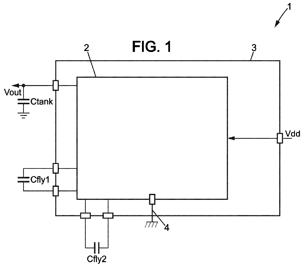
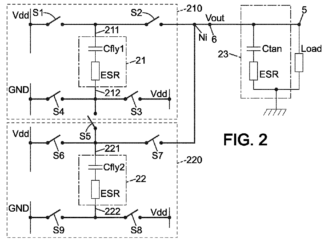
[0064]A multi mode charge pump circuit is described in relation with FIG. 1. Typically, the charge pump circuit comprises a charge pump module 2 in a chip 3 and further external capacitors Cfly1, Cfly2, Ctank. The chip 3 may comprise other modules, designed to perform some operations unrelated to voltage supply. The charge pump circuit 1 comprises an input VDD and a ground connection 4 to connect the charge pump circuit 1 and the chip 3 to the ground. Two of the external capacitors are fly capacitors Cfly1, Cfly2 used as storage units to store a charge during a charging phase and to discharge the accumulated load during a discharging phase. Eventually, the third capacitor is a tank capacitor Ctank arranged to average the output of the charge pump circuit. The tank capacitor is connected by one pin on the output of the chip which is the output of the charge pump circuit and by a second pin to the ground.

[0065]The three capacitors are connected to the chip through a circuit board to w...


PUM


Abstract

There is described a charge pump circuit (1) circuit comprising an input terminal, an output terminal (5) connected to an intermediate node (Ni), a ground terminal (4), a first fly capacitor module (21) with a first fly capacitor (Cfly1) having a first pin (211) and a second pin (212) and connected to the intermediate node (Ni); and a second fly capacitor module (22) with a first fly capacitor (Cfly2) having a first pin (221) and a second pin (222) and connected to the intermediate node (Ni); wherein each being adapted to successively charge and discharge a the first fly capacitor and the second fly capacitor, respectively, wherein the second pin (212) of the first fly capacitor module (21) is connected to the first pin (221) of the second fly capacitor module (22) by a direct connection.

Description

BACKGROUND[0001]1. Technical Field[0002]The present invention generally relates to charge pump circuits. Charge pump circuits are voltage converters that are used in electronic devices such as mobile phones, mobile computers, personal data computers, audio devices and the like.[0003]Charge pump circuits are used in power management circuit in order to replace switched-mode power supply (SMPS) such as boost converters or other DC / DC converters which are expensive due to the cost of an external coil. Thus the same functionality can be achieved with a charge pump circuit which uses only external capacitors.[0004]2. Related Art[0005]Charge pump circuits provide a regulated output voltage from a different input voltage. For instance the charge pump circuit can be arranged to provide a continuous voltage of +5V from an input voltage varying between 3.9V and 2.3V over time. Typical use is when the input voltage is provided by the battery of a mobile device. As the battery gets discharged, ...

Claims


Application Information

Patent Timeline
IPC IPC(8): H02M3/07
CPCH02M3/07Y02B70/1491H02M2001/0054G05F3/00Y02B70/10H02M1/0054H02M3/18
Inventor CHEVALIER, LAURENT
Owner OPTIS CIRCUIT TECH LLC
Why Eureka
Try Eureka