Semiconductor device

a semiconductor and film technology, applied in the direction of semiconductor devices, electrical devices, transistors, etc., can solve the problem of more difficult film processing with high accuracy, and achieve the effect of favorable electrical characteristics and high reliability of semiconductor devices

Inactive Publication Date: 2014-10-30
SEMICON ENERGY LAB CO LTD
View PDF5 Cites 27 Cited by
  • Summary
  • Abstract
  • Description
  • Claims
  • Application Information

AI Technical Summary

Benefits of technology

[0012]Another object of one embodiment of the present invention is to provide a highly reliable semiconductor device. Another object of one embodiment of the present invention is to give favorable electrical characteristics to a semiconductor device including an oxide semiconductor.
[0020]According to one embodiment of the present invention, a semiconductor device that is suitable for miniaturization can be provided. A highly reliable semiconductor device can also be provided. Furthermore, a semiconductor device formed using an oxide semiconductor can have favorable electrical characteristics.

Problems solved by technology

As the shape of a thin film to be processed is minuter, it is more difficult to process the film with high accuracy.

Method used


Image

  • Semiconductor device
  • Semiconductor device
  • Semiconductor device

Examples


embodiment 1

[0039]In this embodiment, a structure and a manufacturing method of a transistor, which is an example of a semiconductor device of one embodiment of the present invention, are described with reference to drawings.

Structural Example

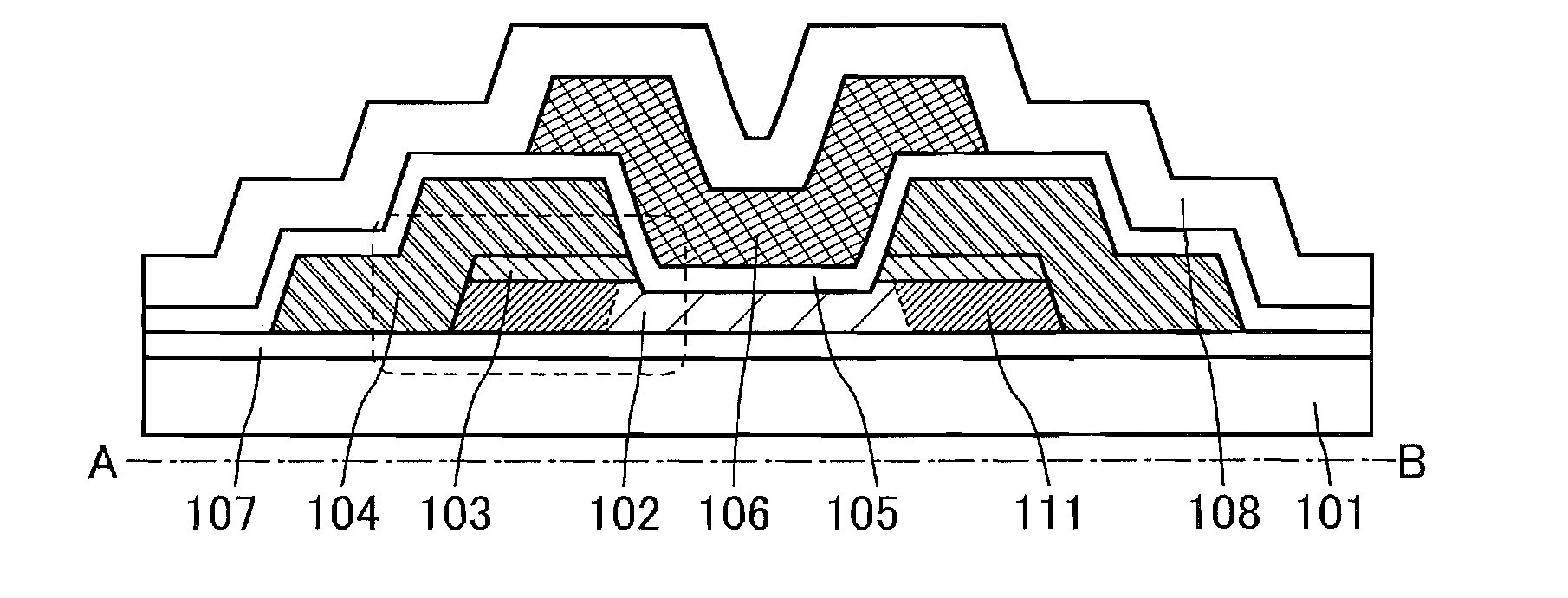
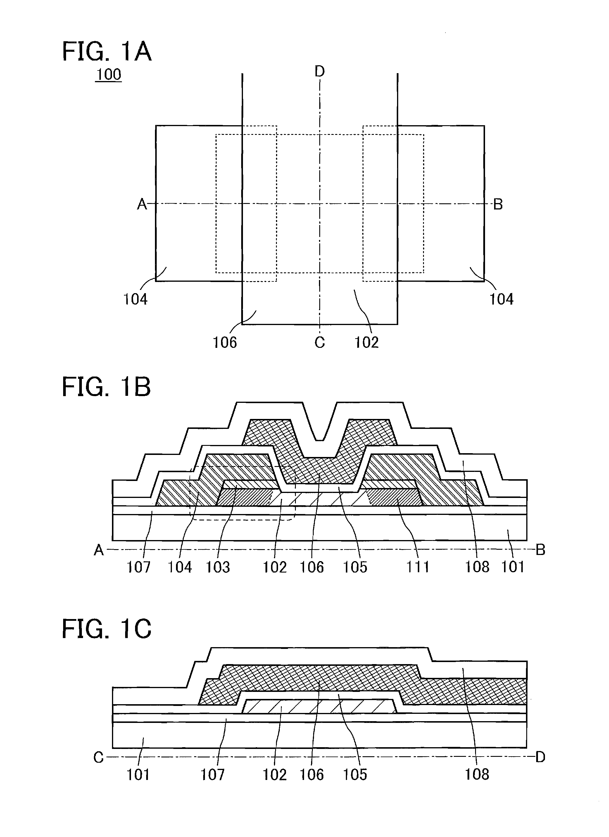
[0040]FIG. 1A is a schematic top view of a transistor 100 described in this structural example. FIGS. 1B and 1C are schematic cross-sectional views taken along the section lines A-B and C-D in FIG. 1A. Some components are not illustrated in FIG. 1A for clarity.

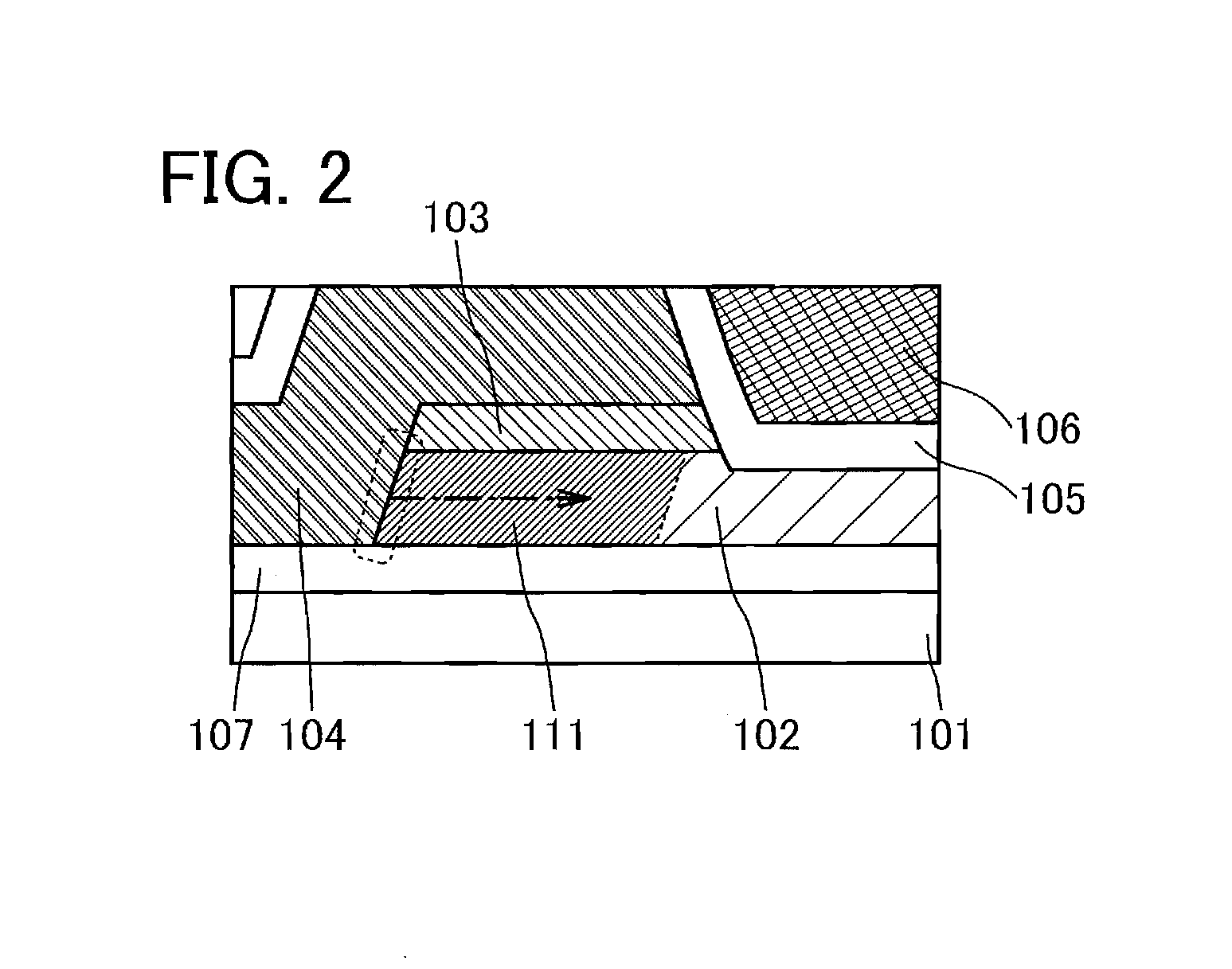
[0041]The transistor 100 is formed over a substrate 101. The transistor 100 includes an island-shaped semiconductor layer 102; a pair of electrodes 104 in contact with the side surfaces of the semiconductor layer 102 and overlapping with a part of the top surface of the semiconductor layer 102; a pair of oxide layers 103 that is located between the semiconductor layer 102 and the electrodes 104 and is in contact with parts of the top surfaces of the semiconductor layer 102 and parts of the bottom sur...

embodiment 2

[0148]An oxide semiconductor that can be favorably used for a semiconductor device of one embodiment of the present invention is described in this embodiment.

[0149]An oxide semiconductor has a wide energy gap of 3.0 eV or more. A transistor including an oxide semiconductor film obtained by processing of the oxide semiconductor in an appropriate condition and having extremely lowered carrier density of the oxide semiconductor can have much lower leakage current between a source and a drain in an off state (off-state current) than a conventional transistor including silicon.

[0150]An applicable oxide semiconductor preferably contains at least indium (In) or zinc (Zn). In particular, In and Zn are preferably contained. In addition, as a stabilizer for reducing variation in electric characteristics of the transistor using the oxide semiconductor, one or more selected from gallium (Ga), tin (Sn), hafnium (Hf), zirconium (Zr), titanium (Ti), scandium (Sc), yttrium (Y), and an lanthanoid (s...

embodiment 3

[0186]In this embodiment, an example of a semiconductor device (memory device) that includes a transistor according to one embodiment of the present invention, that can hold stored data even when not powered, and that has an unlimited number of write cycles will be described with reference to drawings.

[0187]FIG. 7A is a cross-sectional view of the semiconductor device, and FIG. 7B is a circuit diagram of the semiconductor device.

[0188]The semiconductor device illustrated in FIGS. 7A and 7B includes a transistor 3200 including a first semiconductor material in a lower portion, and a transistor 3300 including a second semiconductor material and a capacitor 3400 in an upper portion. Note that the transistor described in Embodiment 1 can be used as the transistor 3300. FIG. 7A illustrates an example where the transistor 100 is used.

[0189]One electrode of the capacitor 3400 is formed using the same material as a source electrode layer and a drain electrode layer of the transistor 3300, t...


PUM


Abstract

To provide a semiconductor device suitable for miniaturization. To provide a highly reliable semiconductor device. To provide a semiconductor device formed using an oxide semiconductor and having favorable electrical characteristics. A semiconductor device includes an island-shaped semiconductor layer over an insulating surface; a pair of electrodes in contact with a side surface of the semiconductor layer and overlapping with a part of a top surface of the semiconductor layer; an oxide layer located between the semiconductor layer and the electrode and in contact with a part of the top surface of the semiconductor layer and a part of a bottom surface of the electrode; a gate electrode overlapping with the semiconductor layer; and a gate insulating layer between the semiconductor layer and the gate electrode. In addition, the semiconductor layer includes an oxide semiconductor, and the pair of electrodes includes Al, Cr, Cu, Ta, Ti, Mo, or W.

Description

BACKGROUND OF THE INVENTION[0001]1. Field of the Invention[0002]One embodiment of the present invention relates to semiconductor devices.[0003]In this specification and the like, the term “semiconductor device” means any kind of device that can function by utilizing semiconductor characteristics, and a transistor, a semiconductor circuit, an arithmetic device, a memory device, an imaging device, an electro-optical device, a power generation device (e.g., a thin film solar cell and an organic thin film solar cell), an electronic appliance, and the like are each one embodiment of semiconductor devices.[0004]2. Description of the Related Art[0005]A technique by which transistors are formed using semiconductor thin films formed over a substrate having an insulating surface has been attracting attention. The transistor is applied to a wide range of electronic appliances such as an integrated circuit (IC) or an image display device (also simply referred to as a display device). As semicon...

Claims


Application Information

Patent Timeline
Patent Type & Authority Applications(United States)
IPC IPC(8): H01L29/786
CPCH01L29/7869H01L29/78618H01L29/41733
Inventor TANAKA, TETSUHIROHANAOKA, KAZUYA
Owner SEMICON ENERGY LAB CO LTD
Why Eureka
Try Eureka