Semiconductor device and method of forming the same

Active Publication Date: 2014-10-30
UNITED MICROELECTRONICS CORP
View PDF7 Cites 6 Cited by
  • Summary
  • Abstract
  • Description
  • Claims
  • Application Information

AI Technical Summary

Benefits of technology

[0006]Accordingly, the present invention provides a method of forming a semiconductor device for suppressing formation of silicon gra

Problems solved by technology

Such silicon grass is undesirable and

Method used


Image

  • Semiconductor device and method of forming the same
  • Semiconductor device and method of forming the same
  • Semiconductor device and method of forming the same

Examples


Embodiment Construction

[0025]Reference will now be made in detail to the present preferred embodiments of the invention, examples of which are illustrated in the accompanying drawings. Wherever possible, the same reference numbers are used in the drawings and the description to refer to the same or like parts.

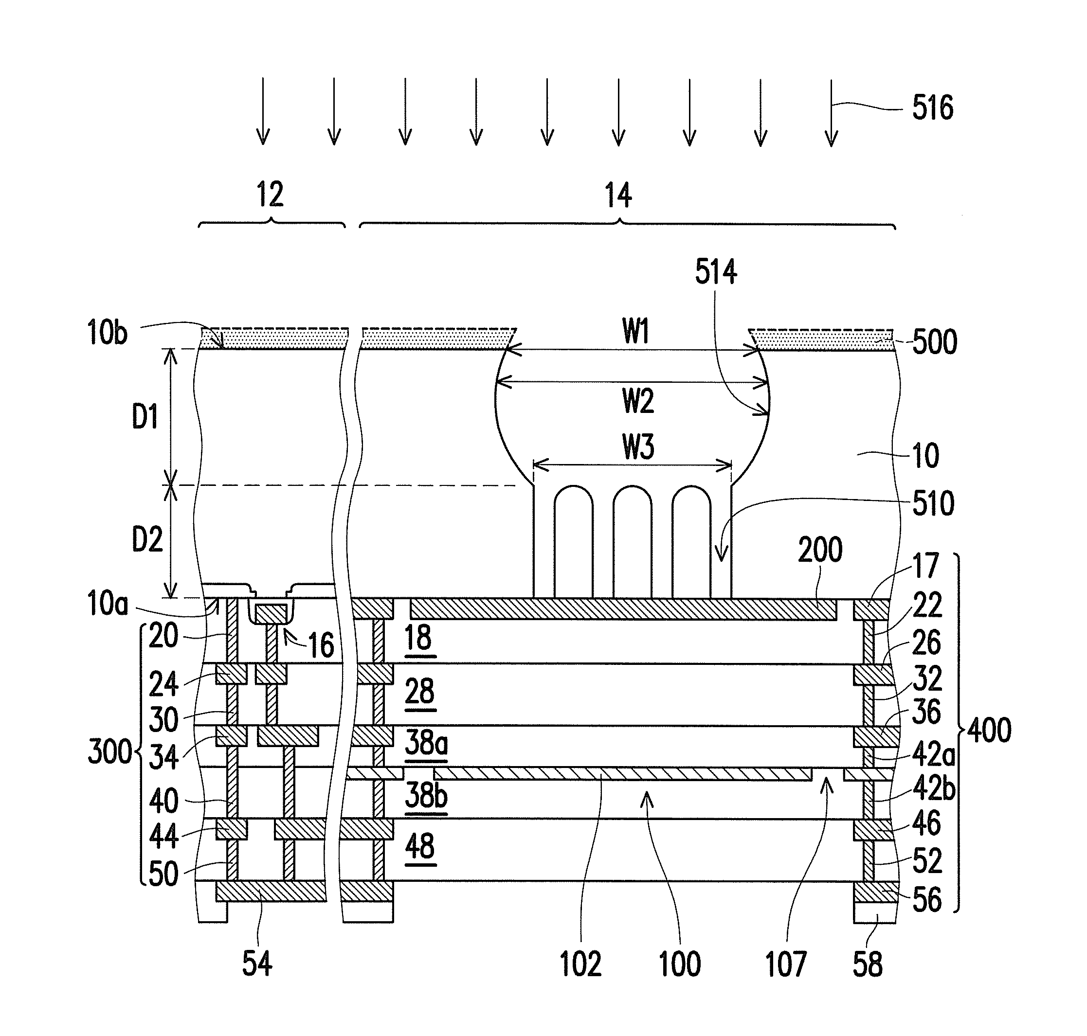
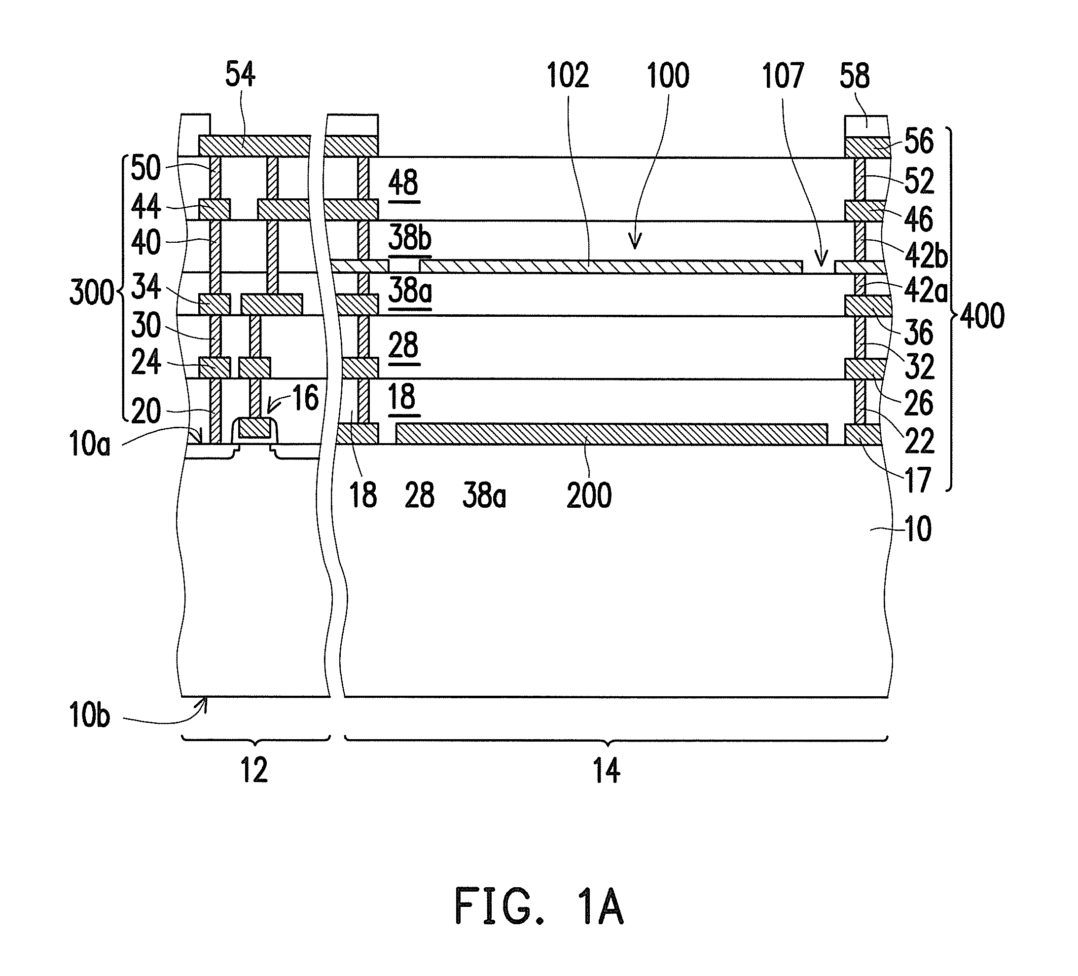
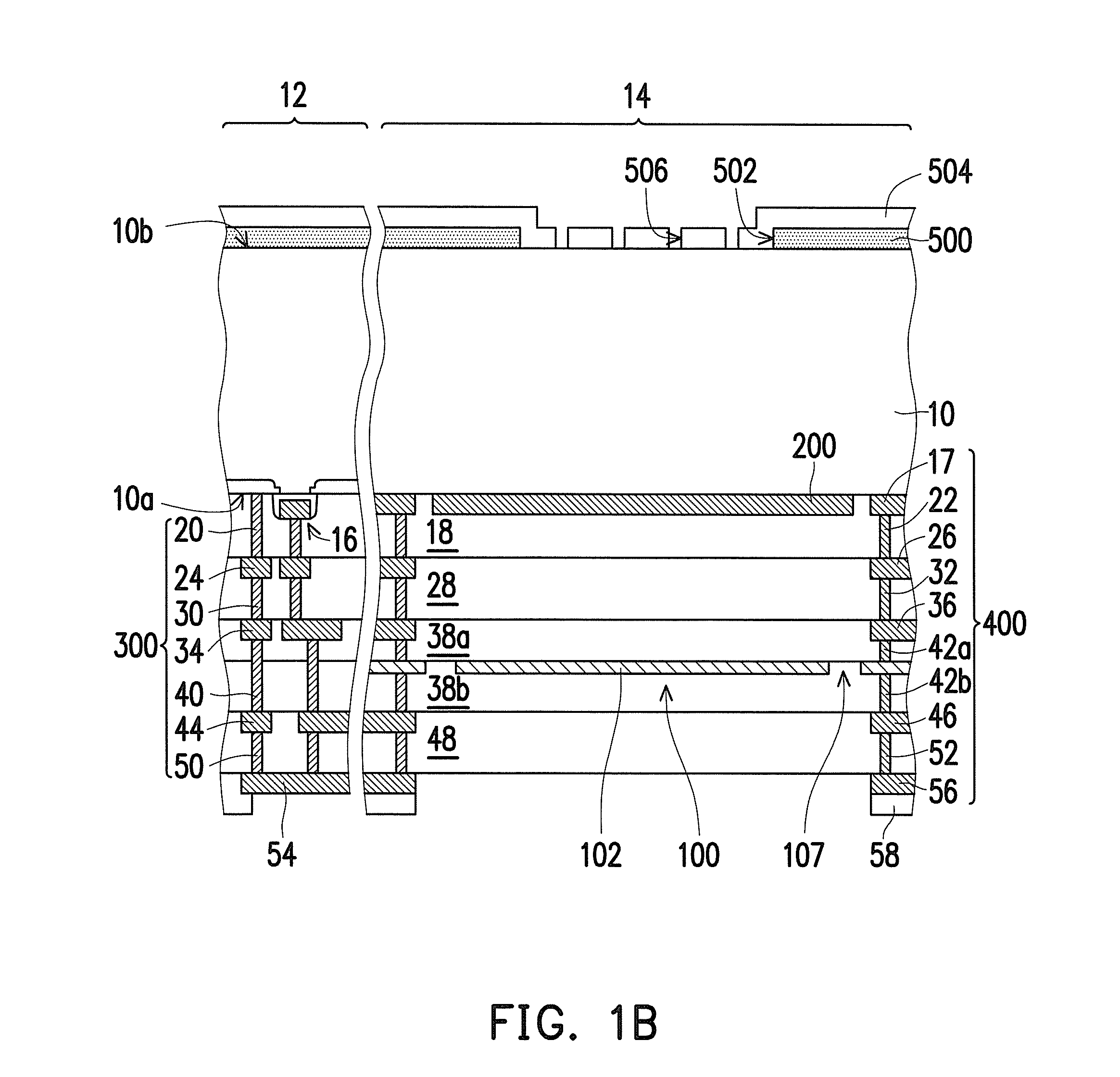
[0026]FIG. 1A to FIG. 1E are schematic cross-sectional views illustrating a method of forming a semiconductor device according to an embodiment of the present invention.

[0027]Referring to FIG. 1A, a substrate 10 having a logic circuit region 12 and a micro-electromechanical system (MEMS) region 14 is provided. The substrate 10 includes a semiconductor material, such as silicon or silicon germanium. The substrate 10 has a first surface 10a and a second surface 10b opposite to the first surface 10a. First, a front-end process is performed to form at least one MOS device 16 on the first surface 10a of the substrate 10 in the logic circuit region 12, and form an electrode 200 and a protection ring 17 on ...


PUM


Abstract

A method of forming a semiconductor device is disclosed. Provided is a substrate having at least one MOS device, at least one metal interconnection and at least one MOS device formed on a first surface thereof. A first anisotropic etching process is performed to remove a portion of the substrate from a second surface of the substrate and thereby form a plurality of vias in the substrate, wherein the second surface is opposite to the first surface. A second anisotropic etching process is performed to remove another portion of the substrate from the second surface of the substrate and thereby form a cavity in the substrate, wherein the remaining vias are located below the cavity. An isotropic etching process is performed to the cavity and the remaining vias.

Description

BACKGROUND OF THE INVENTION[0001]1. Field of Invention[0002]The present invention relates to a semiconductor device and a method of forming the same, and more generally to a semiconductor device having a micro-electromechanical system (MEMS) device and a method of forming the same.[0003]2. Description of Related Art[0004]A MEMS device is a device fabricated by using a micro-machining technique. Due to its advantages of light weight and small size, the MEMS device well satisfies the current requirements for light, thin, short, and small electronic products, and is studied in many fields. The existing MEMS devices include accelerometers, switches, capacitors, sensors, microphones, and other ultra small-sized electromechanical devices.[0005]MEMS microphones fabricated by using the MEMS technique have advantages of light weight, small size, and desirable signal quality, and therefore become the mainstream of miniature microphones. In the process of forming a MEMS microphone, after a MOS...

Claims


Application Information

Patent Timeline
IPC IPC(8): H01L21/311H01L23/48
CPCH01L21/31116H01L23/481H01L2924/0002H01L21/3065B81C2203/0714B81C2203/0742H01L21/76898H04R2201/003B81C1/00246H01L2924/00H01L27/0617
Inventor LIN, MENG-JIAHSU, CHANG-SHENGHUANG, KUO-HSIUNGFANG, WEI-HUAHSIEH, SHOU-WEIWU, TE-YUANLIN, CHIA-HUEI
Owner UNITED MICROELECTRONICS CORP
Why Eureka
Try Eureka