Synthetic diamond coated compound semiconductor substrates

a compound semiconductor substrate and diamond coating technology, applied in the direction of crystal growth process, crystal growth process, chemically reactive gas, etc., can solve the problems of plastic deformation of compound semiconductor substrates, achieve high power density cvd, good cvd diamond growth rate, and high pressure and power density

Active Publication Date: 2014-11-20
AKASH SYST INC
View PDF7 Cites 24 Cited by
  • Summary
  • Abstract
  • Description
  • Claims
  • Application Information

AI Technical Summary

Benefits of technology

[0024]Certain embodiments also use active temperature control to ensure that the temperature across the growth surface is controlled to vary by no more than 80° C., and preferably much less. The present inventors consider that even if the power ramping rate is controlled as described in U.S. Pat. No. 7,939,367, and even if the semiconductor is provided on a thick carrier substrate as described above in accordance with the first aspect of the present invention, warping and plastic deformation of compound semiconductor substrates can still be problematic when operating under high pressure and / or high power density CVD diamond growth conditions. High pressure and power density CVD diamond growth conditions are advantageous to obtain good CVD diamond growth rates and / or good quality polycrystalline CVD diamond material which has very high thermal conductivity. However, such conditions are more problematic in causing plastic deformation of compound semiconductor substrates. As such, the present inventors have developed active temperature control configurations which allow such CVD diamond growth conditions to be utilized while still avoiding the problem of plastic deformation in the compound semiconductor substrate.

Problems solved by technology

However, such conditions are more problematic in causing plastic deformation of compound semiconductor substrates.

Method used


Image

  • Synthetic diamond coated compound semiconductor substrates
  • Synthetic diamond coated compound semiconductor substrates
  • Synthetic diamond coated compound semiconductor substrates

Examples


Embodiment Construction

[0032]As previously described, embodiments of the present invention are based on the realization that a combination of temperature control and substrate rigidity are required in order to eliminate the problem of plastic deformation in compound semiconductor substrates when a CVD diamond layer is grown thereon, particularly when the CVD diamond layer is grown at high pressure / high power conditions to achieve a commercially viable process.

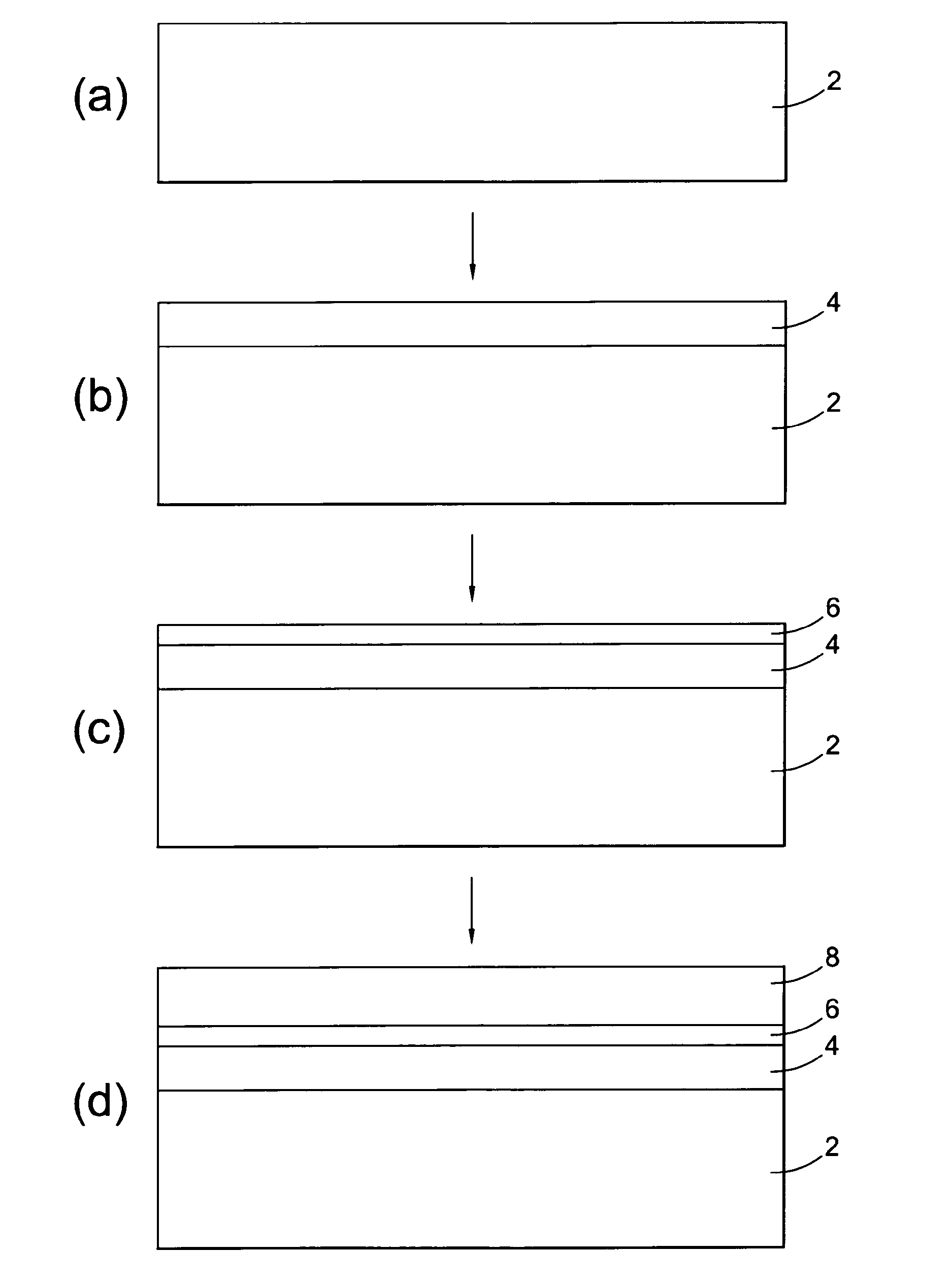
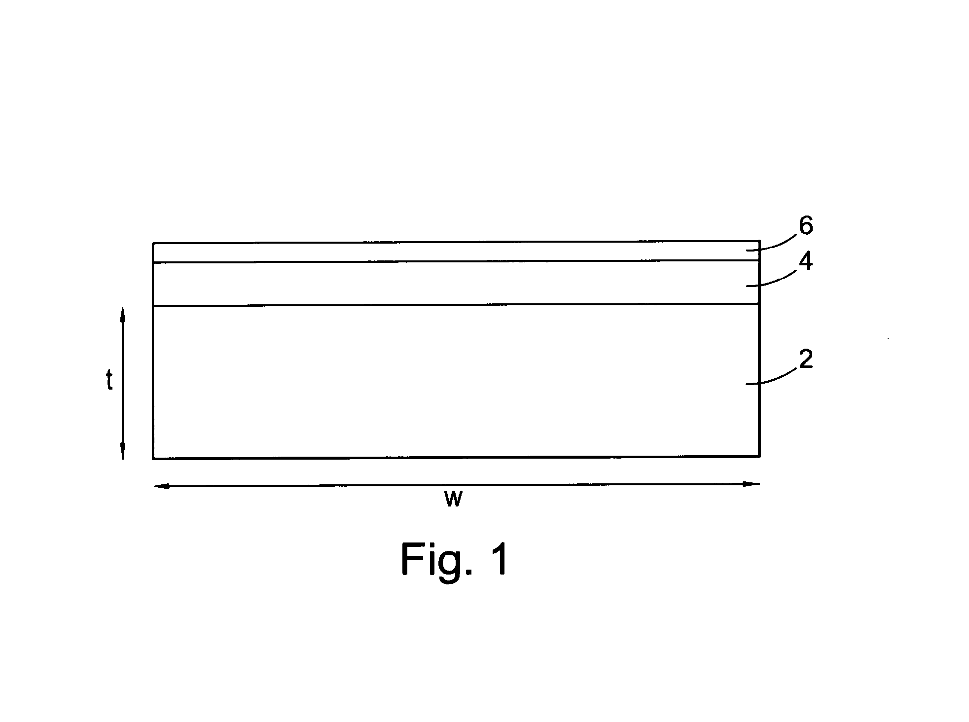
[0033]In light of the above, certain embodiments of the present invention provide a composite substrate as illustrated in FIG. 1. The composite substrate comprising a single crystal carrier wafer 2, a layer of single crystal compound semiconductor 4 epitaxially grown on the carrier wafer 2, and an interface layer 6 disposed on the layer of compound semiconductor 4, the interface layer 6 forming a growth surface suitable for growth of synthetic diamond material thereon via a CVD technique.

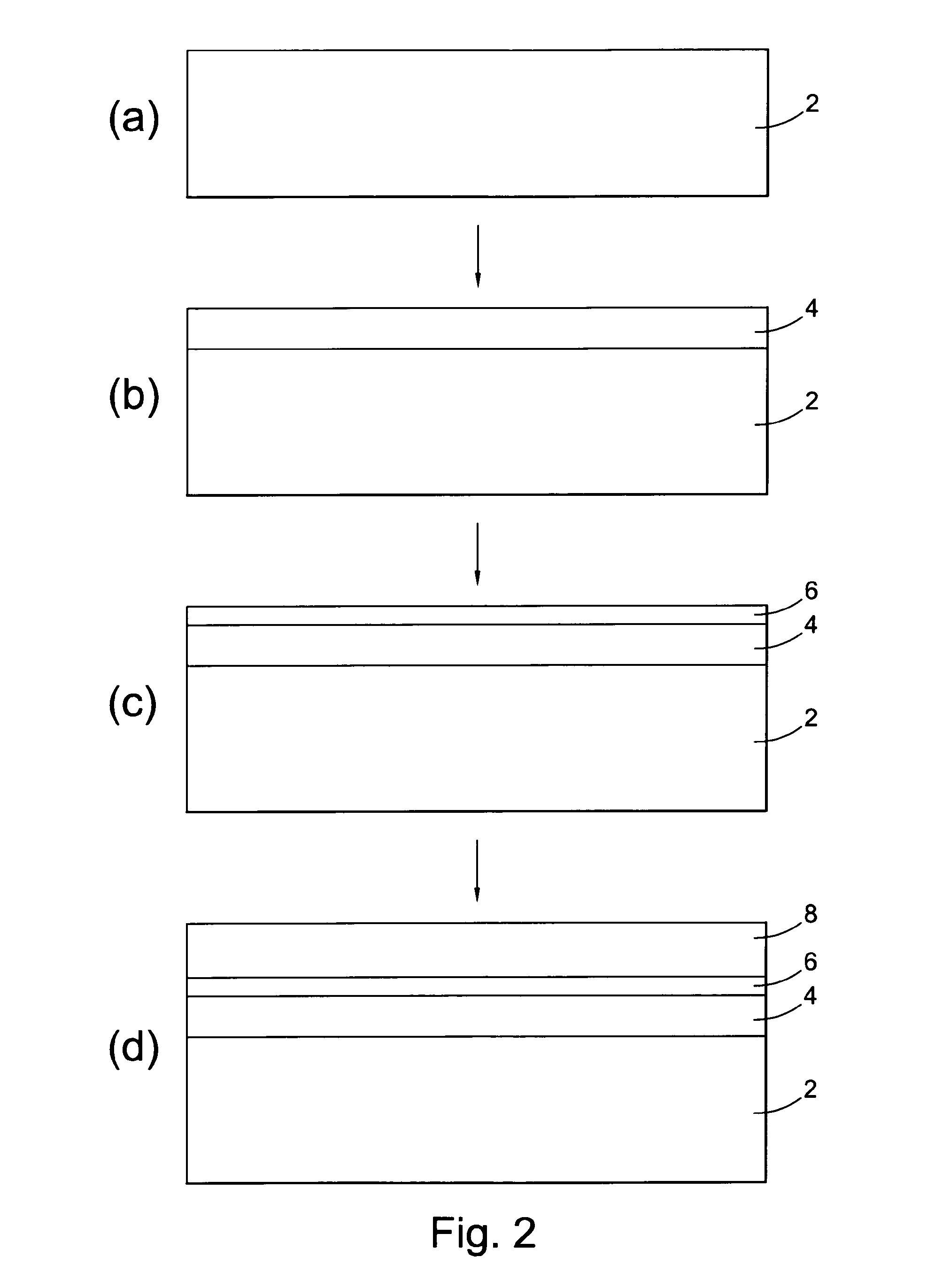
[0034]FIG. 2 illustrates method steps involved in fabricating a...


PUM

PropertyMeasurementUnit
temperatureaaaaaaaaaa
widthaaaaaaaaaa
widthaaaaaaaaaa

Abstract

A method of fabricating a synthetic diamond coated compound semiconductor substrate, the method comprising: loading a composite substrate into a chemical vapour deposition (CVD) reactor, the composite substrate comprising a single crystal carrier wafer, a layer of single crystal compound semiconductor epitaxially grown on the carrier wafer, and an interface layer disposed on the layer of compound semiconductor, the interface layer forming a growth surface suitable for growth of synthetic diamond material thereon via a CVD technique; and growing a layer of CVD diamond material on the growth surface of the interface layer, wherein during growth of CVD diamond material a temperature difference at the growth surface between an edge and a centre point thereof is maintained to be no more than 80° C., and wherein the carrier wafer has an aspect ratio, defined by a ratio of thickness to width, of no less than 0.25/100.

Description

FIELD OF INVENTION[0001]The present invention relates to the manufacture of substrates for semiconductor devices. In particular, embodiments of this invention relate to synthetic diamond coated compound semiconductor substrates and methods of manufacturing the same.BACKGROUND OF INVENTION[0002]Optoelectronic, high power, and high frequency devices are increasingly being fabricated using wide band gap compound semiconductor materials such as gallium nitride, aluminium nitride, and silicon carbide. Such semiconductor materials are frequently grown heteroepitaxially in thin film form onto a suitable substrate which provides a lattice matched template for crystal growth. Typical substrates include sapphire, silicon carbide, and silicon. For semiconductor devices such as microwave amplifier circuits, the substrate should be electrically insulating for the device to function.[0003]A well known problem in semiconductor devices is that of heat dissipation. High temperatures often limit the ...

Claims


Application Information

Patent Timeline
Patent Type & Authority Applications(United States)
IPC IPC(8): H01L21/02H01L23/373
CPCH01L21/02115H01L21/02304H01L21/02271H01L23/3732H01L21/02527C23C16/274C30B29/04H01L21/02447H01L21/0262C30B25/10C30B25/183C23C16/4585C23C16/271H01L2924/0002H01L2924/00H01L33/641
Inventor MOLLART, TIMOTHY PETER
Owner AKASH SYST INC
Why Eureka
Try Eureka