Adhesive Sheet for Semiconductor Wafer Processing, Method for Processing of Semiconductor Wafer Using Sheet

a technology of adhesive sheets and semiconductor wafers, applied in the direction of film/foil adhesives, manufacturing tools, transportation and packaging, etc., can solve the problems of grinding water infiltrating the space, the demand for the properties of above mentioned (1) may not be sufficiently satisfied, and the cost increase, etc., to achieve easy deformation, easy re-releasability, and high aggregation property

Inactive Publication Date: 2014-11-20
LINTEC CORP
View PDF5 Cites 8 Cited by
  • Summary
  • Abstract
  • Description
  • Claims
  • Application Information

AI Technical Summary

Benefits of technology

[0057]In the adhesive layer of the adhesive sheet for the wafer processing of the present invention, the adhesive polymer forms the crosslinked structure, and at least to a part of the crosslinked structure, the polyrotaxane structure is present. That is, the adhesive polymers are indirectly bonded with each other via the structure of polyrotaxane. Therefore, the adhesive layer itself has high aggregation property, and the residues do not remain on the adherend after the releasing of the adhesive sheet. Also, the cyclic molecule in the rotaxane structure has mobility along the linear-chain molecule while being constrained, thus the adhesive agent easily deformed by incorporating into the crosslinked structure, and shows the excellent following property against the roughness of the wafer such as circuit or so, furthermore it is easily re-releasable without the energy ray irradiation or water swelling or so.

Problems solved by technology

However, when using these BG sheet, it is necessary to have special step such as energy ray irradiation or the water swelling of the adhesive layer when releasing, thus the process was complicated and caused the cost increase.
However, the surface of the semiconductor wafer is formed with the roughness such as the circuit and the bumps or so, the adhesive agent having high elasticity has difficulty following such roughness, hence the space is generated, which causes the peeling, and the grinding water may infiltrate from the space in some cases.
That is, the demanded property of above mentioned (1) may not be sufficiently satisfied.
That is, BG sheet using the adhesive agent with the high elasticity has a drawback that it can only be applied to a smooth wafer.
Therefore, the BG sheet which can only be applied to the smooth wafer is failing to respond to the market's demand.
However, when such means are employed, there is a problem that the uncrosslinked component or the plasticizer contaminates the circuit as the residues.
That is, the demanded property of above mentioned (3) may not be sufficiently satisfied.
However, in order to suppress the content of the low molecular weight component as such, it is necessary to strictly control the molecular weight distribution, and requires high levels of technology for the equipment and the production condition or so.
Also, it contains the below problems as well.
However, when the constitution of which the high molecular weight polymer is crosslinked is employed, the elasticity of the adhesive layer rises, and in some case, the roughness following property to the circuit face is deteriorated.
By grinding such backside of such wafer with the bump, the pressure difference caused by the height difference between the parts where the bump is present and the part where the bump is not present directly influences the wafer backside, and it causes a crack or a sink which is called dimple at the wafer backside.
Eventually, this will destroy the semiconductor wafer.
Also, the area where the adhesive layer and the wafer are not in contact occurs at the bottom part of the bumps, which caused the floating or a peeling of BG sheet, and to cause the infiltration of the grinding water.
However, in such constitution, for providing the intermediate layer having different material and production method in addition to the adhesive layer leads to an increase of the steps, and also to the increase of the cost.
However, in order to exhibit a necessary flexibility for the absorbency of the bumps, the aggregation property of the adhesive layer needs to be designed low.
In such case, when releasing the adhesive sheet, the residue tends to easily occur at the adherend surface due to the destruction of the adhesive layer.
On the other hand, if the aggregation property of the adhesive layer is maintained in order to prevent the destruction of the adhesive layer, the projection embedding property tends to decline.
Therefore, for the adhesive sheet having the layer for absorbing the projection only by the adhesive layer, it was extremely difficult to accomplish both contradicting characteristic, which are the suppression of the adhesive agent residue and the absorbency of the projection.

Method used


Image

  • Adhesive Sheet for Semiconductor Wafer Processing, Method for Processing of Semiconductor Wafer Using Sheet

Examples


example 1

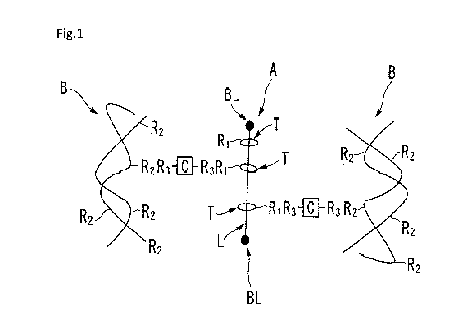
[0152]The adhesive agent mixed with 100 parts by weight of the acrylic based adhesive agent (having butyl acrylate and methyl methacrylate as the main component, and copolymer wherein the content of constituting unit derived from 2-hydroxyethylacrylate is 5 wt %, and the weight average molecular weight of 600,000 the glass transition temperature of −43.6° C., and the solid portion of 40 wt %); 10 parts by weight of the isocyanate based crosslinking agent (BHS-8515, the solid portion of 37.5 wt %, made by TOYO INK CO., LTD); and 9.6 parts by weight of polyrotaxane (SeRM Super Polymer A1000 made by Advanced Softmaterials Inc., the solid portion 35 wt %); was coated on the release material (SP-PET381031 made by LINTEC Corporation) so that the thickness after the drying becomes 40 μm, then dried for 1 minute at 100° C., thereby the adhesive layer was formed on the release material. The exposed face of this adhesive layer was adhered to the low density polyethylene film having the thickn...

example 2

[0154]The adhesive sheet was obtained as same as the example 1, except for using the adhesive agent mixing 100 parts by weight of the acrylic based adhesive agent as same as the example 1, 10 parts by weight of the isocyanate based adhesive agent (BHS-8515 made by TOYO INK CO., LTD), and 3.8 parts by weight of polyrotaxane. Also, Table 1 shows the value of 1+α−β, a relative ratio α of a number of the hydroxyl group of polyrotaxane when the number of the hydroxyl group of the acrylic based adhesive polymer is 1, and a relative ratio β of the number of the isocyanate group of the isocyanate compound when the number of the hydroxyl group of the acrylic based adhesive polymer is 1.

example 3

[0155]The adhesive sheet was obtained as same as the example 1, except for using the adhesive agent mixing 100 parts by weight of the acrylic based adhesive agent as same as the example 1, 8 parts by weight of the isocyanate based adhesive agent (BHS-8515 made by TOYO INK CO., LTD), and 6.1 parts by weight of polyrotaxane. Also, Table 1 shows the value of 1+α−β, a relative ratio α of a number of the hydroxyl group of polyrotaxane when the number of the hydroxyl group of the acrylic based adhesive polymer is 1, and a relative ratio β of the number of the isocyanate group of the isocyanate compound when the number of the hydroxyl group of the acrylic based adhesive polymer is 1.


PUM

PropertyMeasurementUnit
widthaaaaaaaaaa
thicknessaaaaaaaaaa
breaking elongationaaaaaaaaaa

Abstract

To provide an adhesive sheet for wafer processing that satisfies characteristics such as: (1) protecting an uneven circuit surface during grinding with an adhesive force that is not excessively weak; (2) being easy to remove after processing; and (3) leaving very little adhesive residue on the wafer, and that can preferably be used as a removable BG sheet or the like. This adhesive sheet for wafer processing is characterized in having a substrate and an adhesive layer formed on the substrate, the adhesive layer having an adhesive polymer (A) and a polyrotaxane (B) having a linear-chain molecule passing through the opening of the at least two cyclic molecules, and having a block group at both ends of the linear-chain molecule, the adhesive polymer (A) and the cyclic molecule of the polyrotaxane (B) being linked together to form a crosslinked structure.

Description

TECHNICAL FIELD[0001]The present invention relates to the adhesive sheet for semiconductor wafer processing, and further specifically relates to a surface protection sheet for protecting the wafer surface. Also, the present invention relates to the adhesive sheet for the semiconductor wafer processing preferably used for holding the wafer and chips when producing the semiconductor chip by dividing the semiconductor wafer formed with the circuit into each chip.DESCRIPTION OF THE RELATED ART[0002]The electronic devices of recent days put importance on the portability, and has tendency to be thinner and more compact. Also, it is demanded to have higher capacity and faster calculation. Therefore, it has tendency to form a multilayered chip without changing the size of the semiconductor device; and the thinning of the semiconductor wafer for producing the chip which is the constitutional member thereof is in progress. Conventionally, the wafer had the thickness of 350 μm or so, however i...

Claims


Application Information

Patent Timeline
Patent Type & Authority Applications(United States)
IPC IPC(8): H01L21/683H01L21/78C09J7/02H01L21/304C09J7/20
CPCH01L21/6836C09J7/02H01L21/78H01L21/304C09J7/20C08K5/01C09J2203/326H01L2221/68386H01L2221/6834H01L2221/68327C09J2301/408C09J201/02C08G83/007Y10T428/269Y10T428/2852H01L21/30
Inventor TOMINAGA, TOMOCHIKAAKUTSU, TAKASHI
Owner LINTEC CORP
Why Eureka
Try Eureka