

Multicolor LED and Method of Fabricating Thereof
- Summary
- Abstract
- Description
- Claims
- Application Information
AI Technical Summary
Benefits of technology
Problems solved by technology
Method used
Image

Examples
first embodiment
[0042]The present inventors realized that introducing a Group V material limited growth regime, in contrast to the traditional group III limited regime used in III-V growth, ensures that the difference in height of the templates in the first and the second growth areas can be made smaller or even equal. This also means that the total growth area for subsequent layers will be larger in the second growth areas. Therefore, preferably, the templates of the first embodiment are formed through apertures in the growth mask by at least one growth step, such as a at least one metal organic chemical vapor deposition (MOCVD) growth step operating in the Group V material limited growth regime. In this regime, the growth is Group V element (e.g., nitrogen) limited because a relatively low Group V to Group III source gas ratio (e.g., ammonia:TEG or TMG ratio below 1,000, such as 0.001 to 100, for GaN cores) is used. In should be noted that for templates that include both a nanostructure (e.g., na...
second embodiment
[0046]The present inventors realized that increasing local growth area, such as by increasing the density of apertures may increase the height of the densely grown cores further as compared to cores further spaced apart when growing in a group V limited regime. The effect is explained by the V-source, especially and here exemplified by NH3, having a severe kinetic bottleneck in cracking to elemental nitrogen. Approximately 15% NH3 is cracked at 950° C. catalyzed by a GaN surface. A rough estimation of gas phase cracking in the absence of GaN or exposed to a dielectric surface, such as a silicon nitride mask, is 1% to 3% at typical GaN growth temperatures, between 800 and 1000° C. The enlarged surface area of GaN templates formed by a denser spacing of cores can in this way enhance V-limited growth rate and the height of the closer spaced templates well above the height of the templates spaced further apart from each other. This ensures that the total area of the closer spaced templa...
third embodiment
[0048]In this embodiment the heights of the templates in first growth area are preferred to be larger than the height of the templates in the second growth area. This effect can be enhanced by the increase of the GaN surface area in the first growth area, utilizing the kinetic barrier of NH3 cracking as described above. NW core growth step comprised in the template growth in the third embodiment then preferably conducted in the group V material limited growth regime, unless the difference in aperture spacing is much greater than the difference in aperture size between the first and the second areas. In this case, a group III limited growth regime is preferably used. It should be noted that the active region (e.g., QW) and shell growth are preferably conducted in the Group III limited growth regime in all three embodiments irrespective of the regime used to grow the templates.
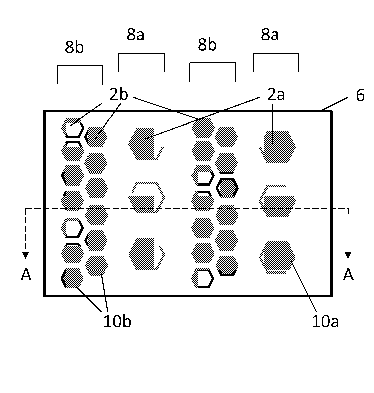
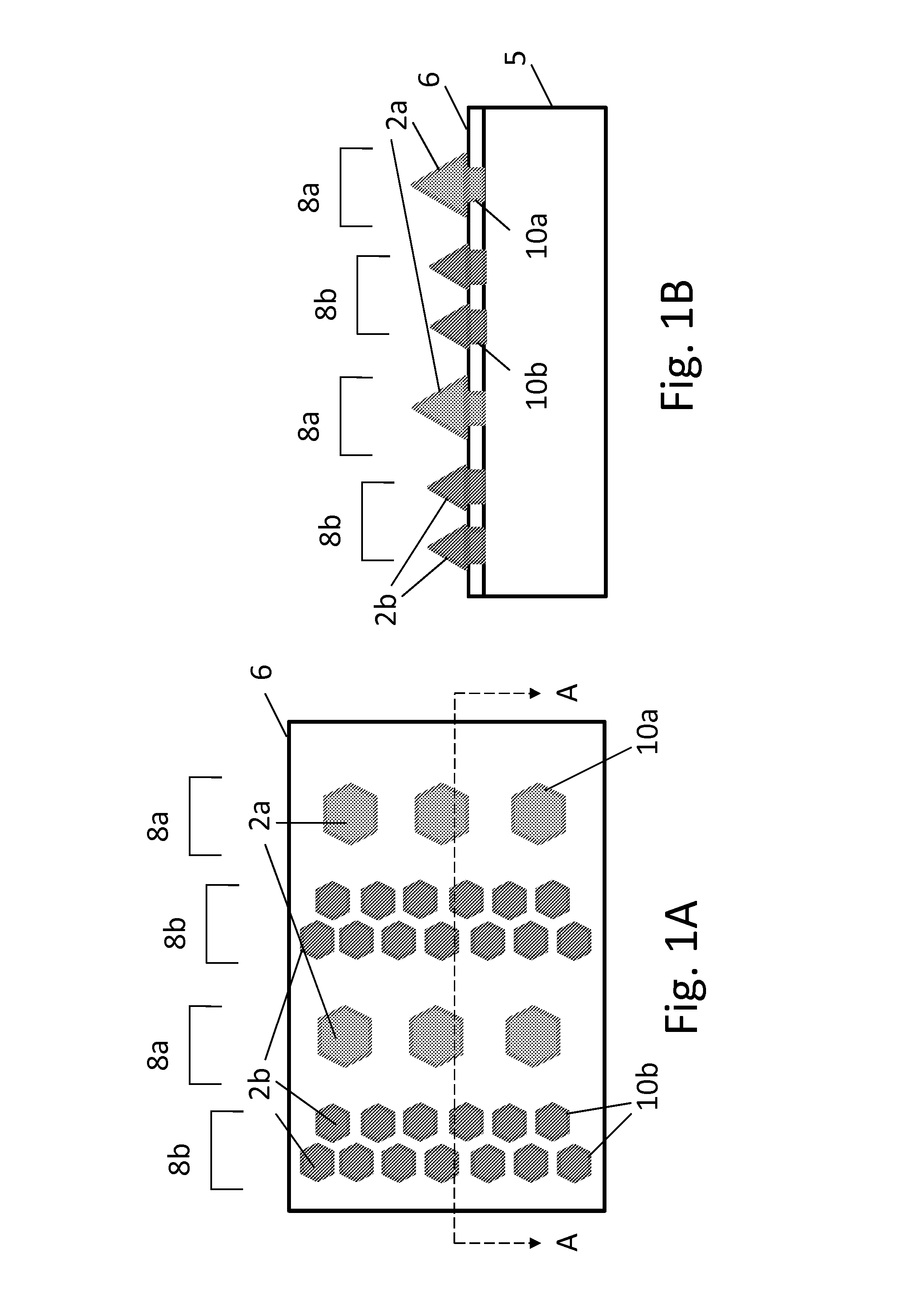
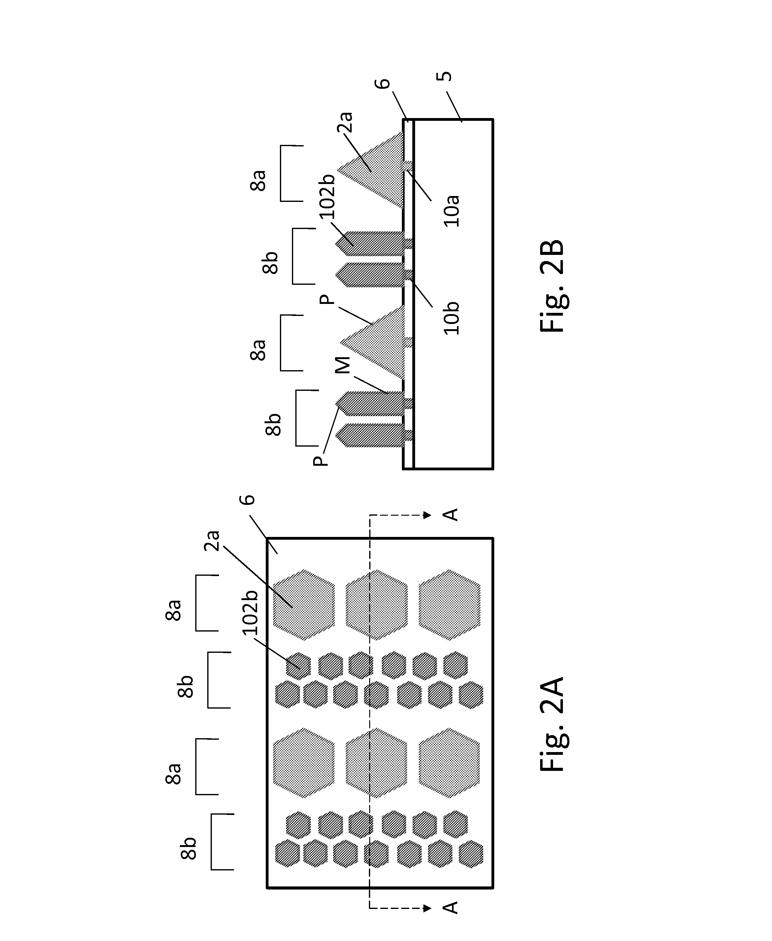
[0049]Thus, the mask used for growing the templates for the LEDs or other optoelectronic devices contains ape...
PUM
 Abstract
Description
Claims
Application Information