Image sensor

a technology of image sensor and chip, applied in the field of image sensor, can solve the problems of deteriorating image quality, degrading image quality, damaging the commercial value of infrared image sensor, etc., and achieve the effect of reducing the thermal stress between the front and the hack surface of the sensor chip

Active Publication Date: 2014-12-18
SUMITOMO ELECTRIC IND LTD
View PDF5 Cites 5 Cited by
  • Summary
  • Abstract
  • Description
  • Claims
  • Application Information

AI Technical Summary

Benefits of technology

[0015]The read-out circuit (silicon) and the sensor chip (compound semiconductor) have thermal expansion coefficients different from each other. In the image sensor according to the present invention, the shielding plate is secured by means of the same resin as the underfill resin to the edge of the sensor chip. In this case, the resin having the same thermal expansion coefficient is applied to both the front and back surfaces of the sensor chip. Therefore, the thermal stress between the front and hack surfaces of the sensor chip can be reduced.

Problems solved by technology

It is found that the image sensor of this type has phenomena (problems) that deteriorate image quality.
Such phenomena seriously degrade the image quality and damage the commercial value of the infrared image sensor.

Method used


Image

  • Image sensor
  • Image sensor
  • Image sensor

Examples


first embodiment

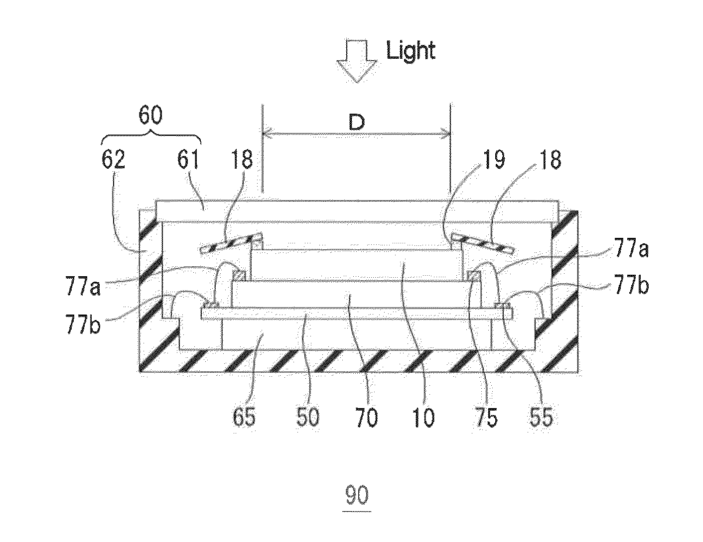
[0035]FIG. 1 is a schematic view of an infrared image sensor 90 according to a first embodiment. In the infrared image sensor 90 illustrated in FIG. 1, a sensor chip 10, a read-out circuit 70, a relay board 50, and a Peltier device 65 are contained in a package 60. The package 60 is made by combining a window 61 with a box-like package main body 62. Since the package 60 may be cooled to a low temperature by using the Peltier device 65 and subjected to a negative pressure, an inert gas, such as nitrogen gas or argon gas, may be sealed in the package 60. A surface of the sensor chip 10 facing the window 61 (typically a back surface of a substrate) is provided with an antireflection coating (AR coating). The sensor chip 10 may be of any type, For example, the sensor chip 10 may include a type-II InGaAs / GaAsSb multi quantum well (MQW) structure formed on an InP substrate as an optical absorption layer, so as to have a sensitivity even in a near-infrared long wavelength region (see FIG. ...

second embodiment

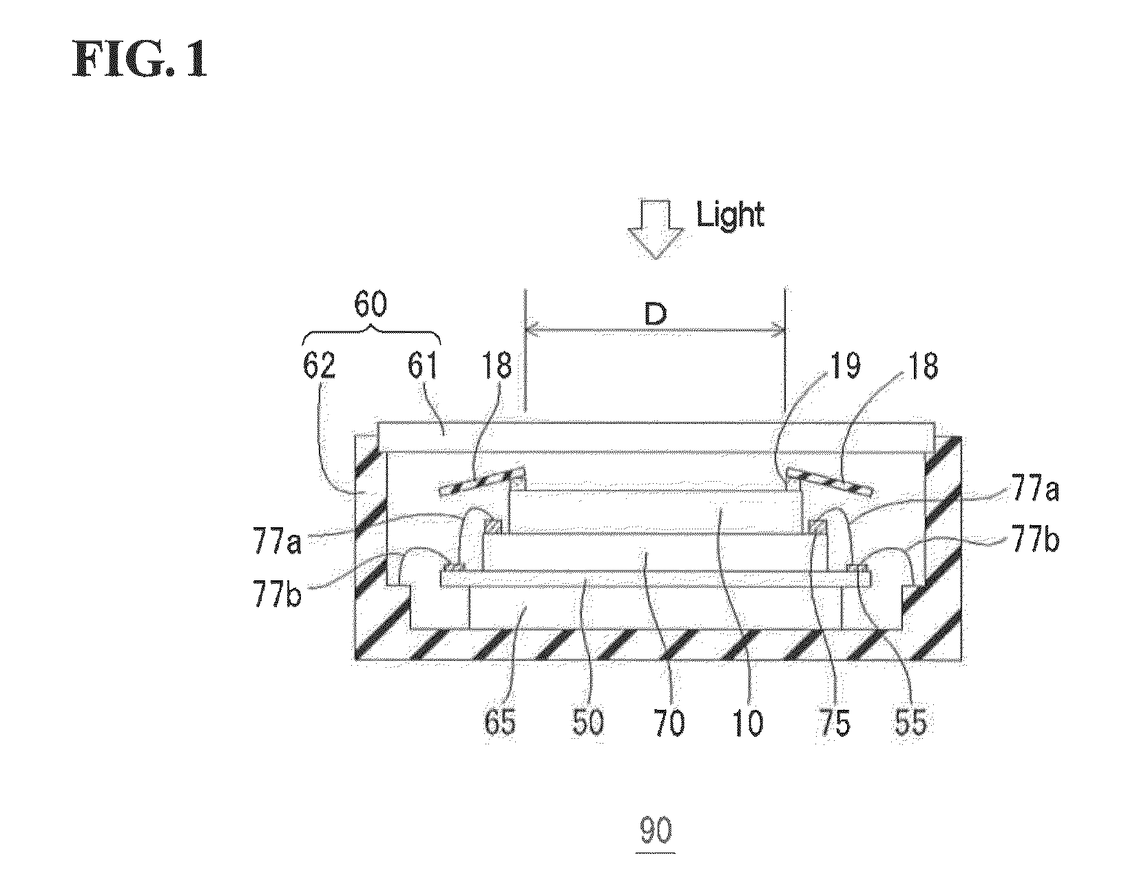
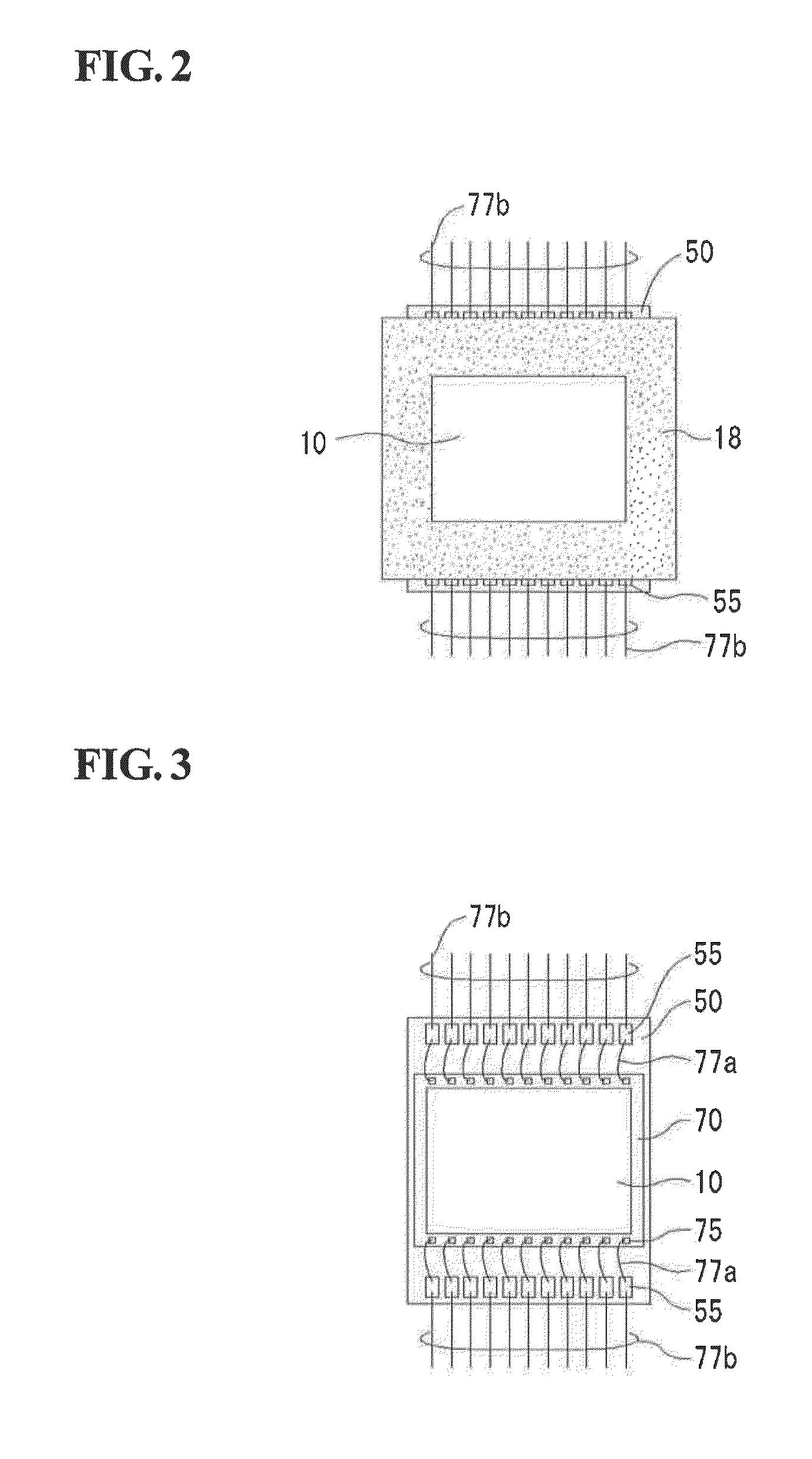
[0042]FIG. 6 is a diagram for explaining an infrared image sensor according to a second embodiment. In the present embodiment, the shielding plate 18 is secured by means of the fixing agent 19 along edges of the relay board 50 where the interconnection electrodes 55 of the relay board 50 are not arranged. The shielding plate 18 may be also secured to the edge of the sensor chip 10. In this embodiment, the shielding plate 18 is secured by using the same resin as the underfill resin 27 as a fixing agent 19, because the resin constituting the underfill resin 27 is resistant to peeling and has high durability. The shielding plate 18 is disposed over the wires 77a and 77b to cover them. FIG. 7 is a plan view of FIG. 6. The shielding plate 18 has a base on the relay board 50. Light traveling off the effective pixel region D is not reflected from the pad electrodes 75 on the CMOS device 70 and the back surface of the window 61 because the light is shielded with the shielding plate 18. In a...

example

[0044]Two test pieces of infrared image sensors including a test piece A1 and a test piece B1 were prepared to examine the uniformity of brightness in an image surface. The test piece A1 is the infrared image sensor 90 illustrated in FIG. 1. The test piece B1 is an infrared image sensor 190 illustrated in FIG. 8. The test piece A1 has the shielding plate 18. The test pieces 131 has the same structure as that of the test piece A1, except that the test piece B1 has no shielding plate. The test pieces A1 and D1 both include the sensor chip 10 and the read-out circuit (CMOS device) 70 illustrated in FIG. 9. As shown in FIG. 9, the sensor chip 10 has a stacked semiconductor layer disposed on an InP substrate 1. The stacked semiconductor layer includes a buffer layer 2, an optical absorption layer 3 having a type-H (InGaAs / GaAsSb) multi quantum well structure, an InGaAs intermediate layer 4, and an InP window layer 5. A plurality of p-type regions 6 are formed by the diffusion of zinc (Zn...


PUM


Abstract

An image sensor includes a package having a window; a sensor chip facing the window, the sensor chip having a pixel region, the sensor chip having an electrode; a read-out circuit disposed farther from the window than the sensor chip, the read-out circuit having a read-out electrode connected to the electrode of the sensor chip; and a shielding plate disposed outside the pixel region of the sensor chip. The shielding plate is configured to block transmission of light.

Description

BACKGROUND OF THE INVENTION[0001]1. Field of the Invention[0002]The present invention relates to an image sensor.[0003]2. Description of the Related Art[0004]Life science-related objects, such as drugs, foods, and living bodies, absorb light of an infrared wavelength range of approximately 1 μm to 3 μm. As the technology in the life science field is developed, the demand for infrared image sensors also increases in the life science field. The infrared image sensors are usually Cooled to, for example, liquid-nitrogen temperature during operation. With improvements in semiconductor technology, infrared image sensors have sufficiently high image quality, even if the infrared image sensors are cooled by using thermoelectric device such as a Peltier device. In addition, the infrared image sensors have become smaller in size. For example, “Two-Dimensional Near Infrared Sensor with Low Noise and Wide Wavelength Range”, SEI TECHNICAL REVIEW, NUMBER 76, pp. 98-101, APRIL (2013) by Yasuhiro I...

Claims


Application Information

Patent Timeline
Patent Type & Authority Applications(United States)
IPC IPC(8): H01L27/146
CPCH01L27/14629H01L27/14618H01L27/14623H01L27/14694H01L2224/48091H01L2224/4911H01L2924/00014
Inventor IGUCHI, YASUHIROINADA, HIROSHIMIGITA, MASAKI
Owner SUMITOMO ELECTRIC IND LTD
Why Eureka
Try Eureka