Electric power conversion circuit

a technology of electric power conversion circuit and control circuit, which is applied in the direction of motor/generator/converter stopper, electronic commutator, dynamo-electric converter control, etc., can solve the problems of incorrect operation of control circuit, dc input terminal switching noise (electromagnetic waves), and incorrect operation of switching elements, so as to reduce noise, suppress the occurrence of incorrect operation, and reduce the effect of switching noise propagation

Active Publication Date: 2014-12-18
DENSO CORP
View PDF1 Cites 6 Cited by
  • Summary
  • Abstract
  • Description
  • Claims
  • Application Information

AI Technical Summary

Benefits of technology

[0013]In the structure of the electric power conversion device according to an exemplary embodiment, the solid pattern is formed in the multi-layer substrate to separate the electronic components and / or the wiring patterns formed on the second surface of the multi-layer substrate from the smoothing capacitor and the conductive members. The formation of the solid pattern can reduce noise propagated from noise generation sources to the electronic components and the wiring patterns. This structure makes it possible to suppress occurrence of incorrect operation of the switching elements and the multi-layer substrate.
[0014]Further, the solid pattern is formed as the interior layer in the inside of the multi-layer substrate. Through the solid pattern, the multi-layer substrate is grounded and electric power is supplied. The subject matter of the present invention uses the solid pattern to reduce switching noise propagated on the second surface of the multi-layer substrate. This structure makes it possible to prevent increase of the overall size of the electric power conversion device and a manufacturing cost.

Problems solved by technology

For example, switching noise (electromagnetic waves) is generated in the DC input terminals when the switching elements are turned on and off.
There is accordingly a possibility of causing incorrect operation in the switching elements when the switching noise is propagated to the control circuit substrate.
However, because noise sources such as the DC input terminals are arranged close to the control circuit substrate in the three phase inverter device having the structure as previously described, the incorrect operation of the control circuit is often caused by switching noise propagated on the control circuit substrate.
Accordingly, this structure increases the manufacturing cost and the whole size of the three phase inverter device.
The problem previously described would be caused in various types of electric power conversion devices such as three phase inverter devices so long as the electric power conversion device performs the switching control operation of the switching elements to convert an input voltage, i.e. a DC voltage to an output voltage, i.e. an alternating current (AC) voltage.

Method used


Image

  • Electric power conversion circuit
  • Electric power conversion circuit
  • Electric power conversion circuit

Examples


first exemplary embodiment

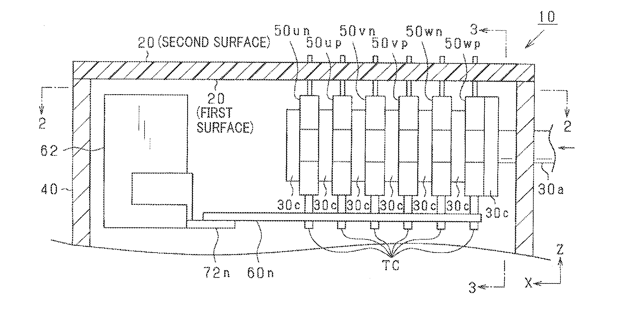
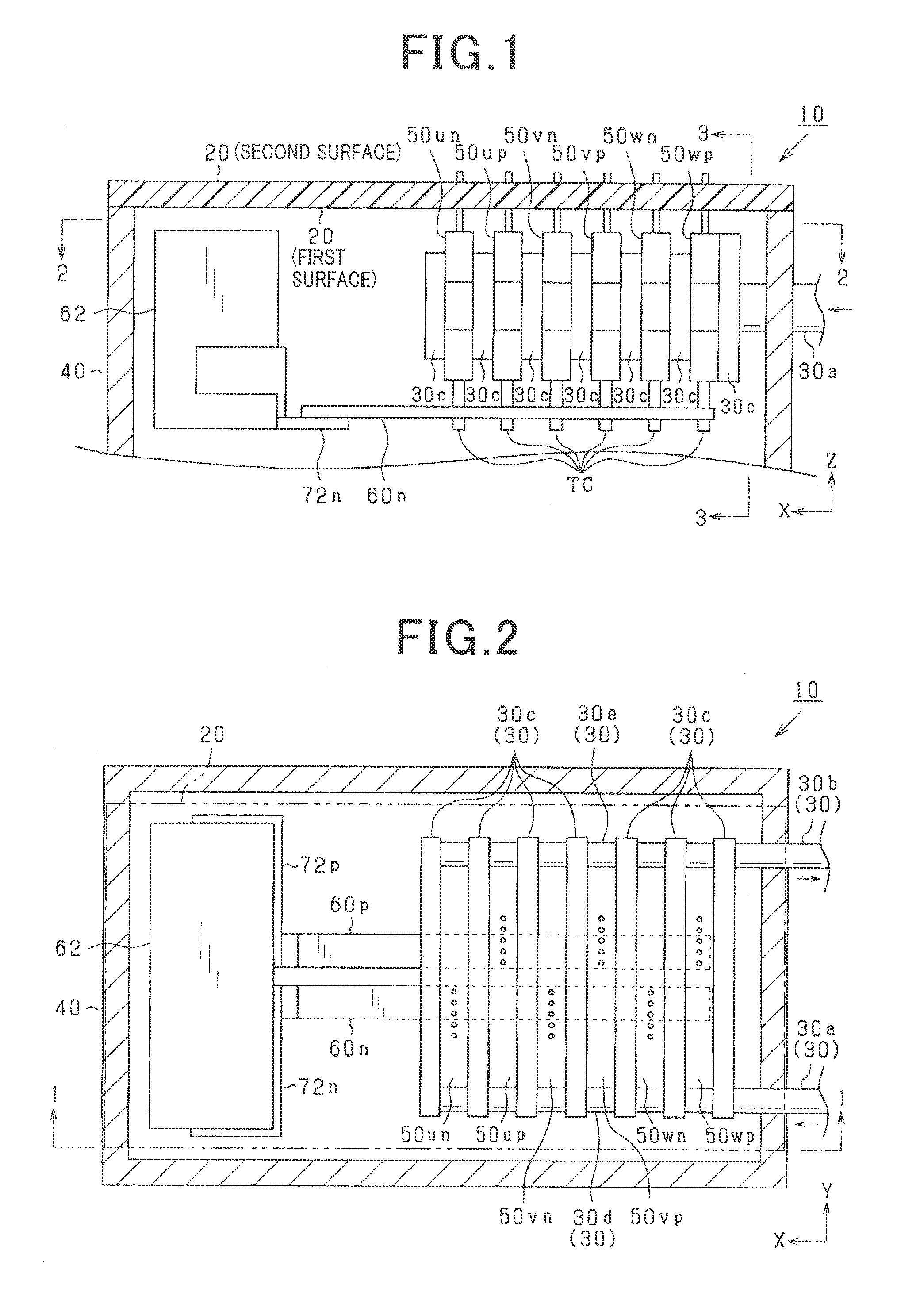
[0044]A description will be given of a three phase inverter device as an electric power conversion device according to a first exemplary embodiment with reference to FIG. 1 to FIG. 22.

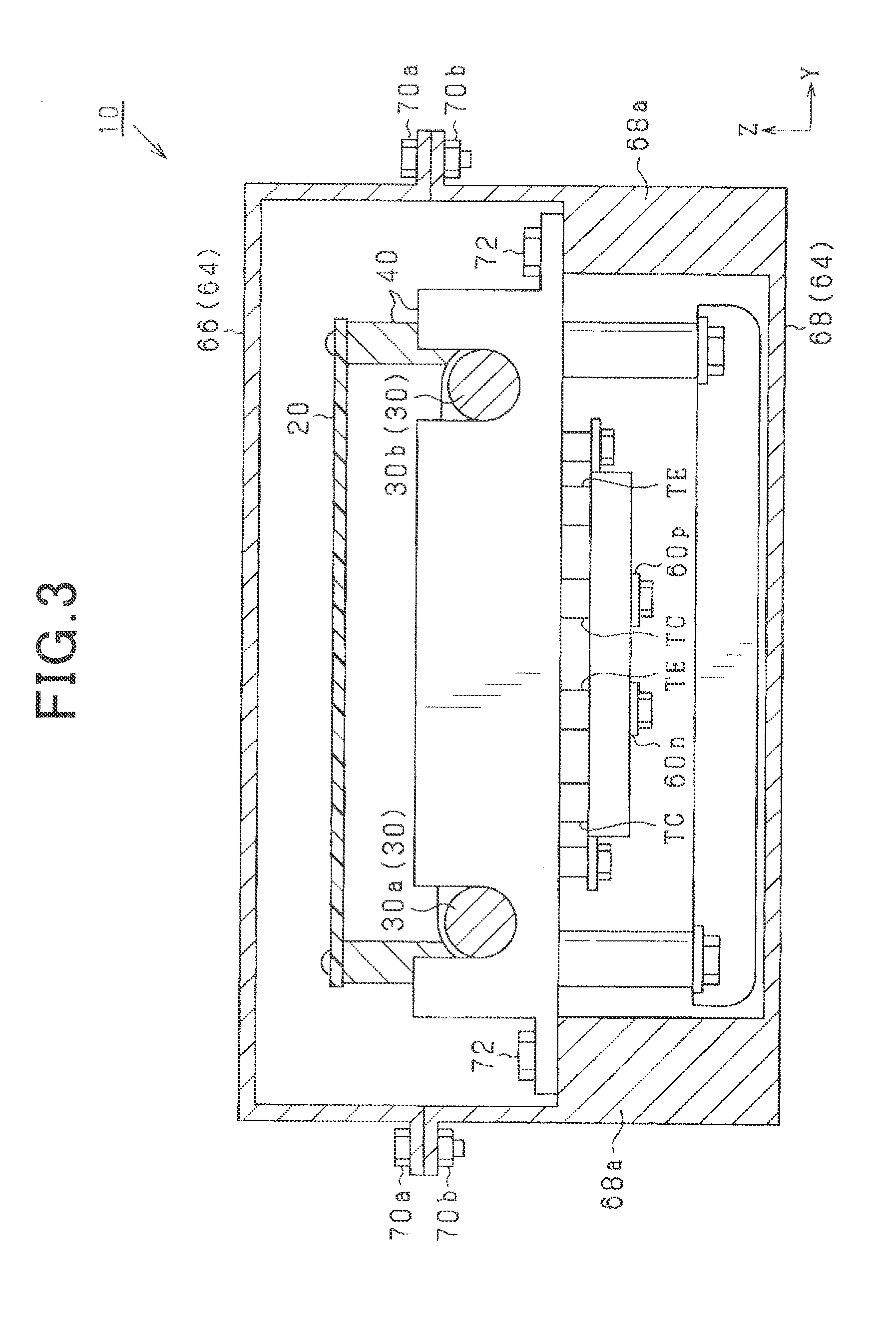
[0045]FIG. 1 is a cross sectional view of the three phase inverter device 10 according to the first exemplary embodiment, along the line 1-1 shown in FIG. 2. FIG. 2 is a cross sectional view of the three phase inverter device 10 along the line 2-2 shown in FIG. 1. FIG. 3 is a cross sectional view of the three phase inverter device 10 along the line 3-3 shown in FIG. 1.

[0046]A description will now be given of a whole structure of the three phase inverter device 10 according to the first exemplary embodiment with reference to FIG. 1, FIG. 2 and FIG. 3.

[0047]As shown in FIG. 1, FIG. 2 and FIG. 3, the three phase inverter device 10 is comprised of a circuit substrate 20 (or a multi-layer substrate) having a multi-layer structure, a cooling device 30, a frame 40, semiconductor modules 50up, 50un, 50vp, 50vn...

second exemplary embodiment

[0149]A description will be given of the three phase inverter device as the electric power conversion device according to a second exemplary embodiment with reference to FIG. 23 and FIG. 24.

[0150]FIG. 23 is a plan view showing the circuit substrate 20, when observed from the second surface side (at the smoothing capacitor 62 side), used in the three phase inverter device according to the second exemplary embodiment. FIG. 24 is a plan view showing the circuit substrate 20-1, when observed from the first surface side, used in the three phase inverter device according to the second exemplary embodiment.

[0151]As shown in FIG. 23 and FIG. 24, a differential wiring pattern 130a (made of copper foil, for example) is formed in the first surface of the circuit substrate 20. FIG. 23 is a plan view showing the circuit substrate 20 when observed from the second surface side (the housing casing 64 side). On the other hand, FIG. 24 is a plan view showing the circuit substrate 20 when observed fro...

third exemplary embodiment

[0155]A description will be given of the three phase inverter device 10 as the electric power conversion device according to a third exemplary embodiment with reference to FIG. 25, FIG. 26 and FIG. 27.

[0156]The three phase inverter circuit 10 according to the third exemplary embodiment has two sub-smoothing capacitors, i.e. a first smoothing capacitor 63a and a second smoothing capacitor 63b.

[0157]A description will now be given of the overall structure of the three phase inverter device 10 according to the third exemplary embodiment with reference to FIG. 25, FIG. 26 and FIG. 27.

[0158]The same components between the third exemplary embodiment and the first and second exemplary embodiments will be referred to with the same reference numbers and characters for brevity.

[0159]FIG. 25 is a cross sectional view of the three phase inverter device 10 according to the third exemplary embodiment, along the line 5-5 shown in FIG. 26. FIG. 26 is a cross sectional view of the three phase inver...


PUM


Abstract

In a three phase inverter device, a smoothing capacitor, a bus bar at a positive electrode side and a bus bar at a negative electrode side are formed on a first surface of the circuit substrate. Electronic s components containing a microcomputer, etc., a differential wiring pattern, a single wiring pattern and a current wiring pattern are formed on a second surface of the circuit substrate. A ground pattern is formed in the inside of the circuit substrate in order to separate the electronic components, the differential wiring pattern, the single wiring pattern and the current wiring pattern from the smoothing capacitor, the bus bar at the positive electrode side and the bus bar at the negative electrode side.

Description

CROSS-REFERENCE TO RELATED APPLICATION[0001]This application is related to and claims priority from Japanese Patent Application No. 2013-123908 filed on Jun. 12, 2013, the contents of which are hereby incorporated by reference.BACKGROUND OF THE INVENTION[0002]1. Field of the invention[0003]The present invention relates to electric power conversion devices such as inverter devices comprised of switching elements and a control circuit for performing a turning-on and off control of the switching elements.[0004]2. Description of the Related Art[0005]A patent document 1, Japanese patent laid open publication No. 2012-139016, has disclosed a three phase inverter device. The three phase inverter device is comprised of switching elements, for example, insulated gate bipolar transistors (IGBTs), a control circuit substrate, direct current (DC) input terminals, a smoothing capacitor and a housing casing. A control circuit is mounted to the control circuit substrate. The control circuit contro...

Claims


Application Information

Patent Timeline
Patent Type & Authority Applications(United States)
IPC IPC(8): H02M7/537H02P6/08H02M7/48H02P29/00H05K3/46
CPCH02P6/08H02M7/537H02M7/003H02P21/06H02M7/00
Inventor MIYACHI, JYUNJIMAEBARA, TSUNEOASAKO, YOUSUKE
Owner DENSO CORP
Why Eureka
Try Eureka