Semiconductor integrated circuit having a MPU and a DRAM cache memory

a technology integrated circuit, which is applied in the direction of transistors, basic electric elements, instruments, etc., can solve the problems of increased chip size of lsi and malfunction in the operation of dram cache memory

Inactive Publication Date: 2002-04-23
NEC ELECTRONICS CORP
View PDF3 Cites 15 Cited by
  • Summary
  • Abstract
  • Description
  • Claims
  • Application Information

AI Technical Summary

Benefits of technology

It is another object of the present invention to provide a semiconductor integrated circuit which is capable of reducing the noise propagated from the overlying interconnect lines extending between the bonding pads and the MPU to the word lines or data lines formed as the underlying metallic interconnect lines.
It is a further object of the present invention to provide a semiconductor integrated circuit which is capable of reducing the noise propagated from the MPU to the data line of the DRAM cache memory through the source lines.
In accordance with the LSI of the present invention, by providing two-layer source lines, the underlying source line providing operating current for the DRAM macro block is less affected by the potential fluctuation of the overlying source line which is caused by the microprocessor having a higher power dissipation.

Problems solved by technology

This increases the chip size of the LSI.
Moreover, if the noise generated on the overlying interconnect lines, especially on the source line, extending between the bonding pads and the MPU is propagated through the parasitic capacitance to the word lines or the data lines disposed below the overlying interconnect lines, a malfunction may arise in the operation of the DRAM cache memory.

Method used


Image

  • Semiconductor integrated circuit having a MPU and a DRAM cache memory
  • Semiconductor integrated circuit having a MPU and a DRAM cache memory
  • Semiconductor integrated circuit having a MPU and a DRAM cache memory

Examples


Embodiment Construction

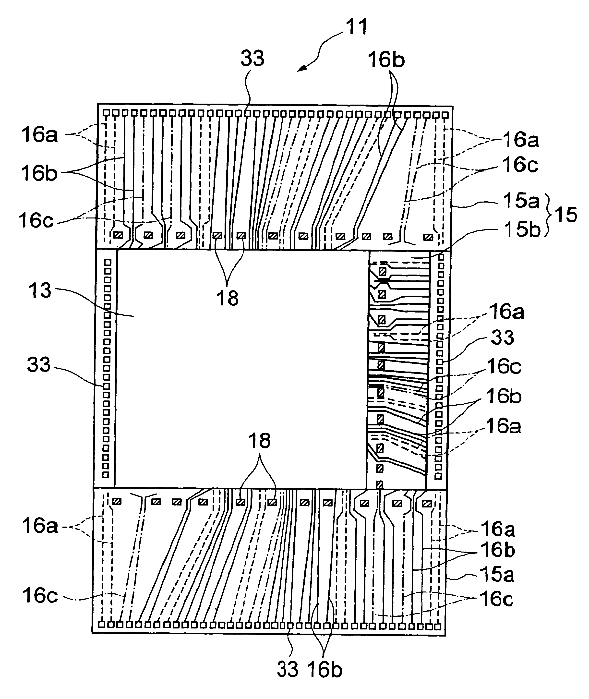
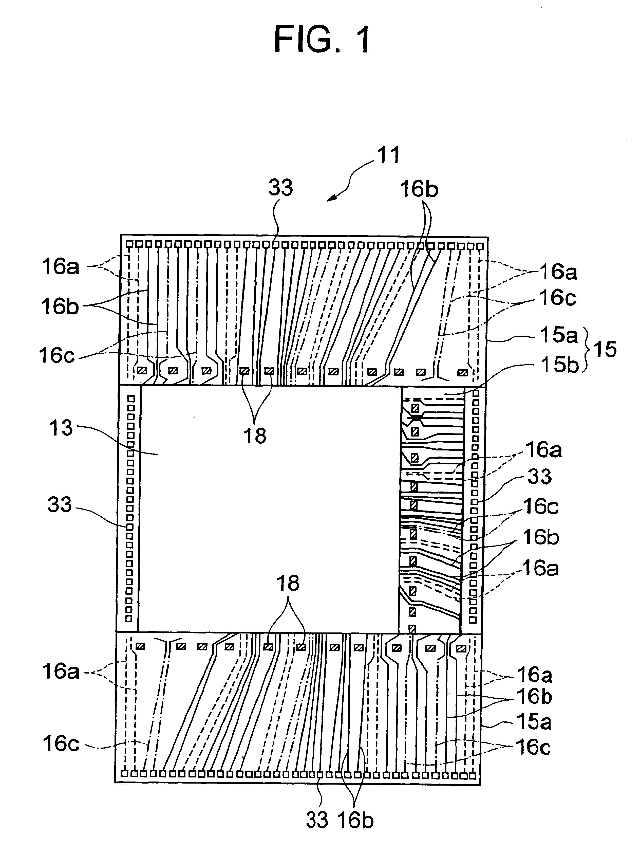
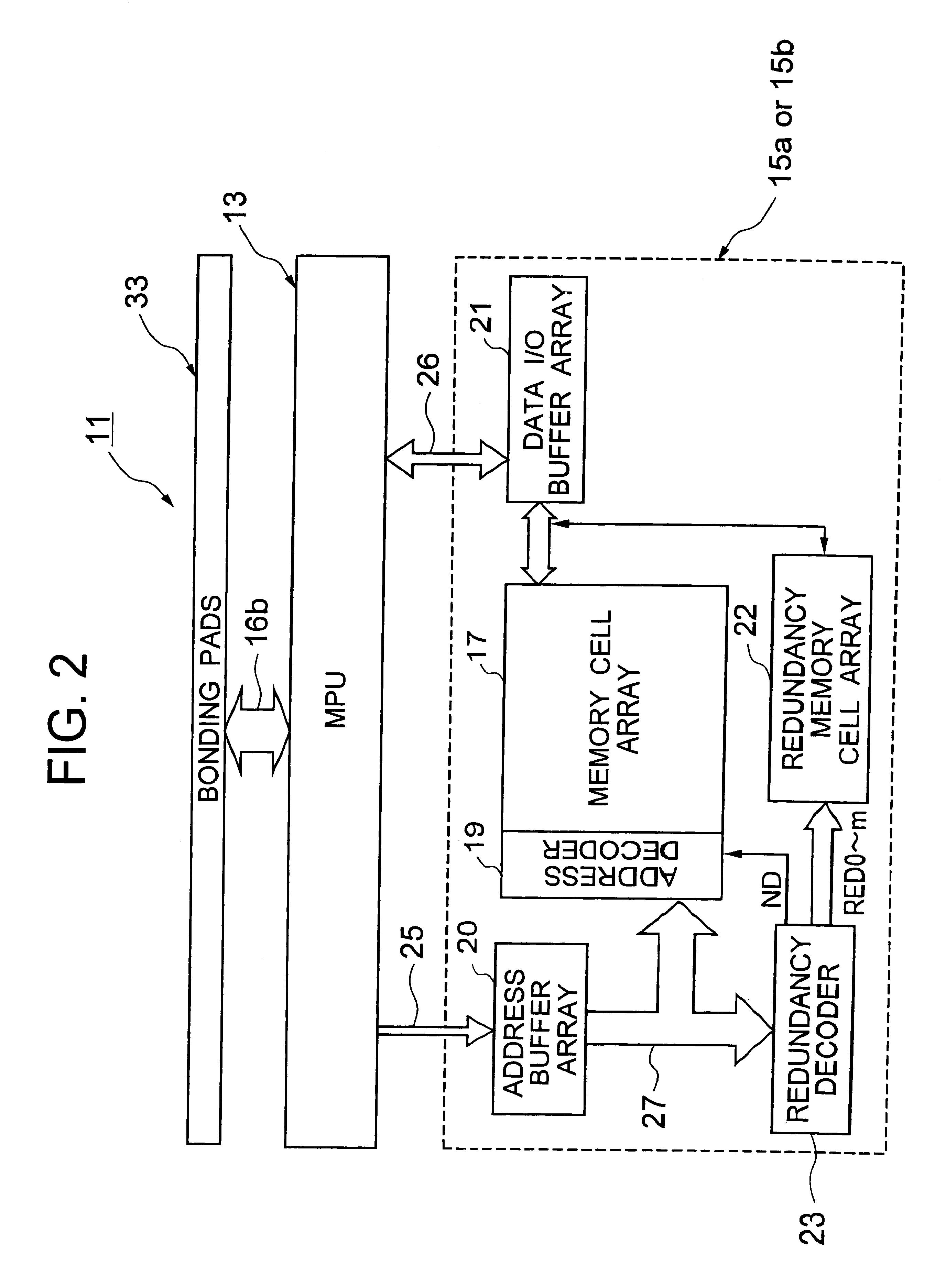
Referring to FIG. 1, an LSI 11 according to an embodiment of the present invention includes a MPU 13 located in a central area of the chip, a DRAM cache memory 15 including three DRAM macro blocks 15 and 15b disposed at the peripheral area of the chip for surrounding the MPU 13 at three sides thereof, and bonding pads 33 disposed in the vicinity of four edges of the chip.

The DRAM macro blocks include a pair of cache data macro blocks 15a, and a tag data macro block 15b, each of which has a redundancy function. The bonding pads 33 disposed in the vicinity of three edges of the chip are disposed in opposite to the MPU 13 with an intervention of the DRAM macro blocks 15a and 15b, whereas the bonding pads 33 disposed in the vicinity of the remaining edge are disposed adjacent to the MPU 13. The number of bonding pads 33 is 600, for example. The arrangement of the LSI is not depicted to any accuracy of scale.

Interconnect lines 16 depicted in the drawing includes source lines 16a for supp...


PUM


Abstract

A large scale semiconductor integrated circuit, implemented on a chip, includes an MPU and a DRAM cache memory including a plurality of DRAM macro blocks located around the MPU. The DRAM macro block has a redundancy function for which a plurality of fuses are disposed for cut-out by laser beams. The lower metallic layers implement source lines for power and ground to the DRAM macro blocks, whereas a topmost metallic layer implements source lines for the MPU. The topmost metallic layer circumvents areas of the chip where portions of a metallic layer constituting fuses for implementing the redundancy function are located.

Description

(a) Field of the InventionThe present invention relates to a semiconductor integrated circuit having a micro processing unit (microprocessor) and a DRAM cache memory on a single chip and, more particularly, to the structure of interconnect lines disposed on the chip.(b) Description of the Related ArtIn view of a low operational speed of a main storage device used for a micro processing unit (MPU) in a computer system, it is usual that the MPU is associated with a cache memory having a higher operational speed. The cache memory temporarily stores some of data for the MPU to compensate the low speed of the main storage device.In general, the cache memory devices, required to have a higher operational speed, have been implemented by static random access memories (SRAMs), which generally have a larger circuit scale per unit capacity however. Thus, a small-capacity SRAM is generally used heretofore for the cache memory.It is desirable that a dynamic random access memory (DRAM) having a l...

Claims


Application Information

Patent Timeline
Patent Type & Authority Patents(United States)
IPC IPC(8): H01L23/52H01L23/528H01L21/70G11C29/00H01L23/525H01L21/8242G11C11/401H01L21/3205H01L21/82H01L21/822H01L27/04H01L27/10H01L27/108
CPCH01L23/5286G11C29/80H01L23/5258H01L27/10894H01L2924/0002H01L2924/00H10B12/09H01L27/10
Inventor SUGIBAYASHI, TADAHIKO
Owner NEC ELECTRONICS CORP
Why Eureka
Try Eureka