

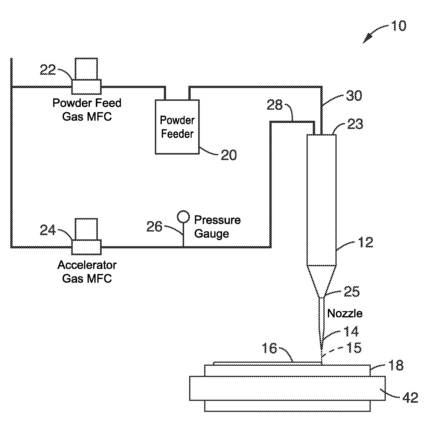
Micro cold spray direct write systems and methods for printed micro electronics
a technology of direct write and micro-electronics, applied in the direction of conductive pattern formation, combustion types, lighting and heating apparatus, etc., can solve the problems of increasing manufacturing costs, unable to print conductive features smaller than 50 m consistently, and unsuitable for low-cost flexible electronic devices. achieve the effect of small siz
- Summary
- Abstract
- Description
- Claims
- Application Information
AI Technical Summary
Benefits of technology
Problems solved by technology
Method used
Image

Examples
experiment # 1
[0046]Experiment #1 Setup
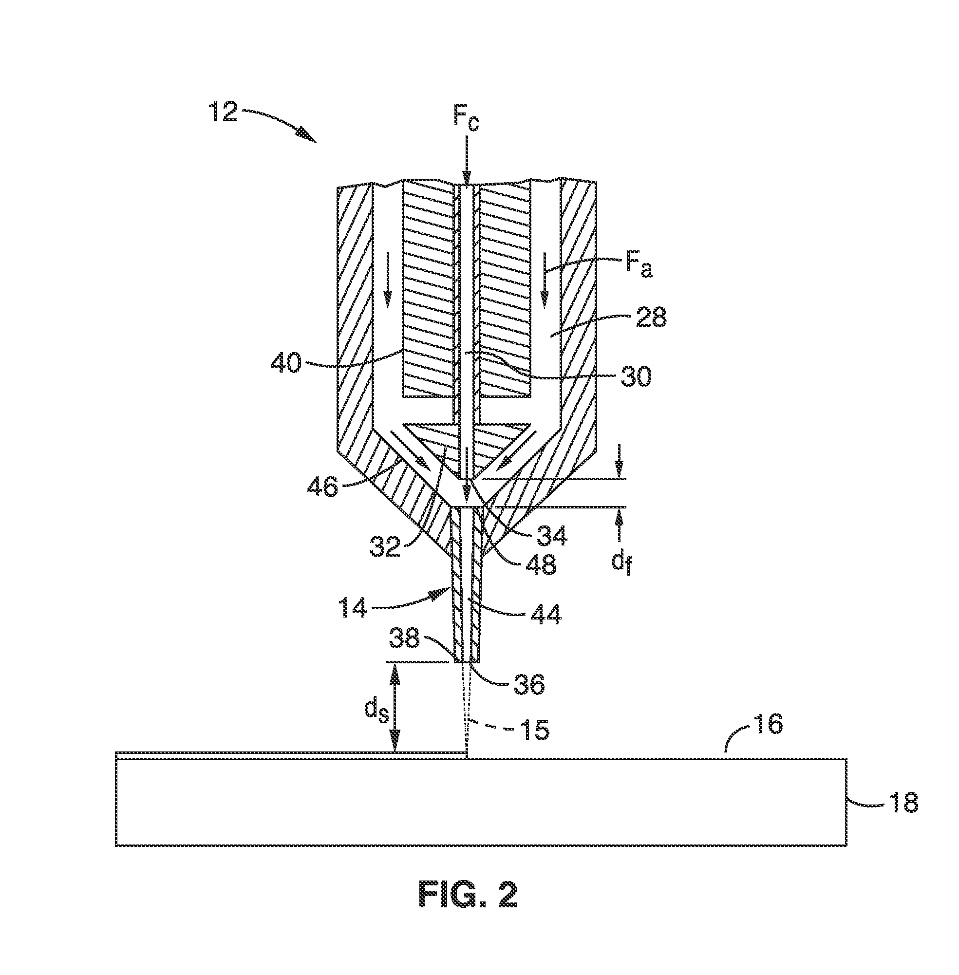
[0047]Two prototype MCS deposition heads were built. A first prototype test MCS deposition head built without a flow cone, and one built with a flow cone 32 as illustrated in FIG. 2. It was shown that introduction of the flow cone in the second prototype demonstrated a significant decrease in feature size and overspray in lines printed. A linearly converging nozzle 14, as depicted in FIG. 2, with an inlet 48 diameter of 1 mm, exit or throat diameter of 200 μm, and length of 19 mm was used for this set of experiments. For varying the gauge pressure, the carrier gas flow rate was kept constant at 800 cm3 / minute and the accelerator gas flow rate was varied between 2200 cm3 / minute to 14000 cm3 / minute which resulted in a gauge pressure at inlet 48 of the nozzle 14 of 50 psi to 90 psi.
[0048]Using appropriate deposition conditions, copper, aluminum and tin particles with size varying between 0.5 μm-5 μm were deposited on glass substrates. The average height of the ...
experiment # 2
[0063]Experiment #2 Setup
[0064]One challenge that arises from interpreting experimental results is the difficulty in knowing the exact particle size. To reduce this unknown, a powder feeder was incorporated that uses a high velocity gas jet in combination with an electromagnetic actuator to feed powder at flow rates as low as 40 ccm, with a mass of powder as small as 250 mg. For this work, 3.8 μm nominal diameter near-spherical silica powder (Cospheric Inc., Santa Barbara Calif., USA, part # SiO2MS-4 um) which has a CV<10% and a 99% degree of roundness was used. An SEM image of the silica particles is shown in FIG. 11. It is evident that these particles indeed are both near spherical, and about 4 μm in diameter. In some instances, the particles appear to have flattened features, but this is merely a consequence of the conductive carbon tape used to secure the particles for imaging.
[0065]Experiment #2 Results
[0066]FIG. 12 show a plot of results of beam width measurements for both a t...
PUM
| Property | Measurement | Unit |
|---|---|---|
| width | aaaaa | aaaaa |
| width | aaaaa | aaaaa |
| width | aaaaa | aaaaa |
Abstract
Description
Claims
Application Information