Circuit substrate and manufacturing method thereof

a technology of circuit substrate and manufacturing method, which is applied in the direction of synthetic resin layered products, metal layered products, domestic applications, etc., can solve the problems of high pore ratio of woven materials, inability to disclose the method of getting good adhesion between the surface of glass film and the resin layer, and destruction of electronic products, etc., to achieve good adhesion

Inactive Publication Date: 2014-12-25
GUANGDONG SHENGYI SCI TECH
View PDF0 Cites 2 Cited by
  • Summary
  • Abstract
  • Description
  • Claims
  • Application Information

AI Technical Summary

Benefits of technology

[0006]The object of the present invention is to provide a circuit substrate, wherein a porous glass film is used as carrier material, causing the resin adhesion layer has good binding force with the glass film surface.
[0007]Another object of the circuit present invention is to provide a circuit substrate manufactured by using the porous glass film, wherein the number of pores in the glass film is controlled to make the glass accounts for more than 45% in volume based the whole glass film, causing the CTE in either X or Y direction of the circuit substrate reduced compared with prior art.
[0008]A further object of the present invention is to provide a method for manufacturing a circuit substrate, wherein a porous glass film is used as the carrier material. The method has good formability and convenient operation.
[0030]first, using a porous glass film as carrier material make the adhesion layer has good binding force with the glass film surface, because the resin can enter the pores of the glass film and plays the role of pins;
[0031]second, controlling the number of pores in the glass film to make the glass accounts for more than 45% by volume based on the whole glass film, causing the CTEs in X, Y and Z directions of the circuit substrate reduced compared with the copper clad laminate using glass fiber fabric as reinforcing material in the prior art;
[0032]third, the manufacturing process of the circuit substrate of the present invention is simple and thus easy to apply to a large-scale production.

Problems solved by technology

Nevertheless, as the glass fiber fabric is limited by manufacturing process, the woven material has a high pore ratio.
Said patent application disclosed a multi-layer board structure was composed of a glass film, a resin layer and a copper layer, however, it did not disclose how to get good adhesion between the surface of the glass film and the resin layer.
This further causes that the copper clad laminate manufactured by this method has low reliability during PCB fabrication, PCB element assembly and use of electronic products, leading to destroy of electronic products.

Method used


Image

  • Circuit substrate and manufacturing method thereof
  • Circuit substrate and manufacturing method thereof

Examples


example 1

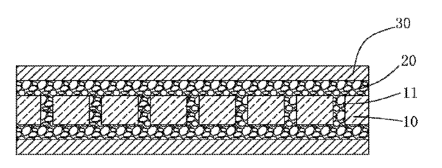
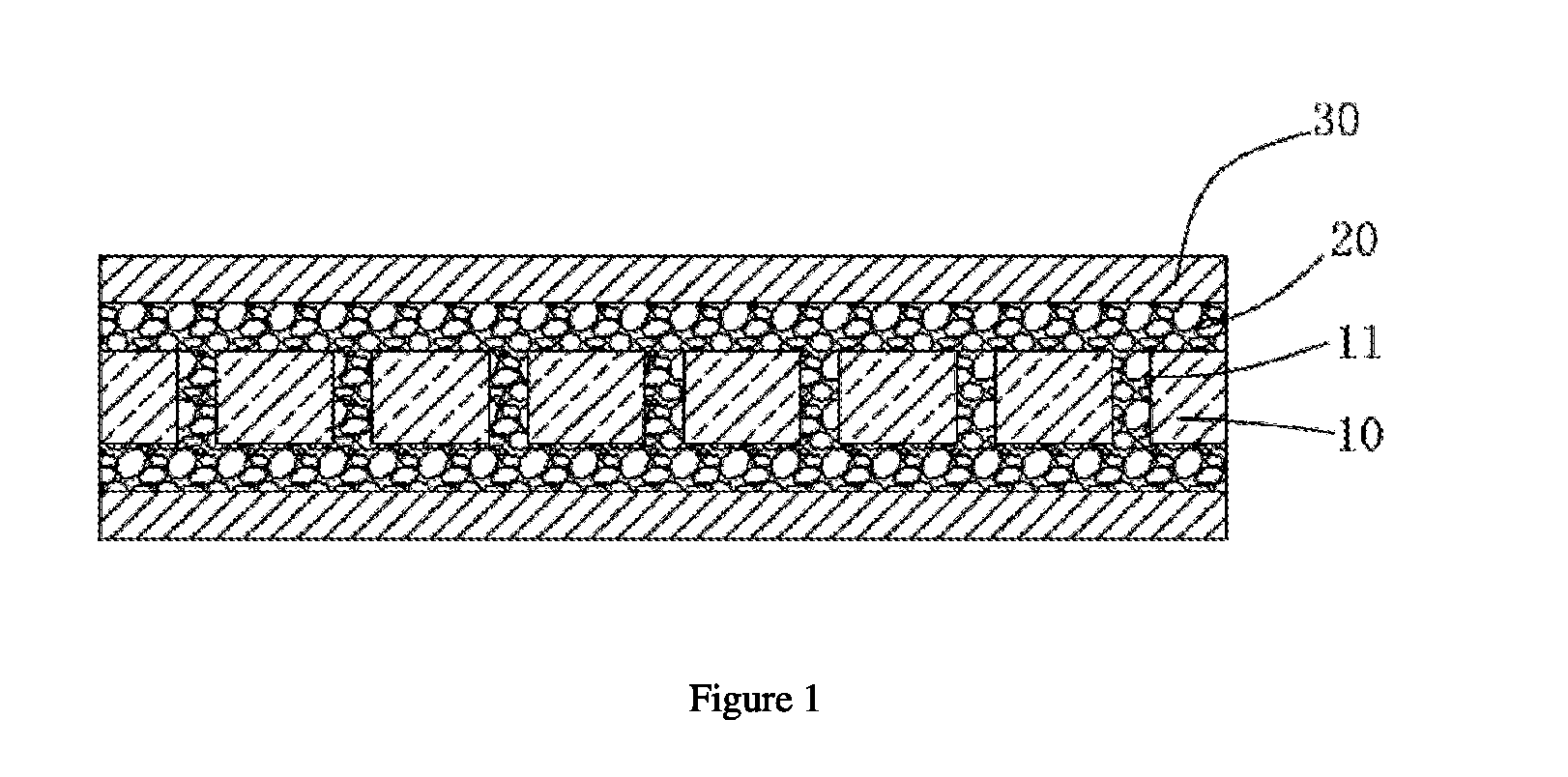
[0065]Take a porous glass film with thickness of 200 μm, pore diameter of 100 μm, and glass volume percentage of 65% (dried and pre-treated with a coupling agent), on each side of the glass film put a FR4 prepreg (that is, prepreg used for S1141 copper clad laminate of Guangdong Shengyi Sci. Tech Co., Ltd.) manufactured by impregnating a glass fibre fabric having a thickness of 0.1 mm (2116 glass fibre fabric) into epoxy resin glue system (dicyandiamide curing agent) and conduct laminating; then on each sides put a copper foil and conduct laminating again.

[0066]Put the above-mentioned laminated layers into a presser machine at a curing temperature of 180° C. and a curing pressure of 15 Kg / cm2 in vacuum. Conduct hot pressing to obtain a circuit substrate (that is, copper clad laminate). Test the circuit substrate: the peel strength between the copper foil and the prepreg is 1.7 N / mm and that between the prepreg and the glass film is 1.2 N / mm; the CTEs before reaching the glass-transi...

example 2

[0067]Take a porous glass film with thickness of 50 μm, pore diameter of 20 μm, and glass volume percentage of 80% (dried and pre-treated with a coupling agent), on each side of the glass film put a FR4 prepreg (that is, prepreg used for S1141 copper clad laminate of Guangdong Shengyi Sci. Tech Co., Ltd.) manufactured by impregnating a glass fibre fabric having a thickness of 0.06 mm (1080 glass fibre fabric) into epoxy resin glue system and conduct laminating; then on each sides put a copper foil and conduct laminating again.

[0068]Put the above-mentioned laminated layers into a presser machine at a curing temperature of 180° C. and a curing pressure of 15 Kg / cm2 in vacuum. Conduct hot pressing to obtain a circuit substrate (that is, copper clad laminate). Test the circuit substrate: the peel strength between the copper foil and the prepreg is 1.7 N / mm and that between the prepreg and the glass film is 0.8 N / mm; the CTEs before reaching the glass-transition temperature is 7.1 ppm / ° ...

example 3

[0069]Take a porous glass film with thickness of 1 mm, pore diameter of 200 μm, and glass volume percentage of 50% (dried and pre-treated with a coupling agent), on each side of the glass film put a FR4 prepreg (that is, prepreg used for S1141 copper clad laminate of Guangdong Shengyi Sci. Tech Co., Ltd.) manufactured by impregnating a glass fibre fabric having a thickness of 0.06 mm (1080 glass fibre fabric) into epoxy resin glue system (dicyandiamide curing agent) and conduct laminating; then on each sides put a copper foil and conduct laminating again.

[0070]Put the above-mentioned laminated layers into a presser machine at a curing temperature of 180° C. and a curing pressure of 25 Kg / cm2 in vacuum. Conduct hot pressing to obtain a circuit substrate (that is, copper clad laminate). Test the circuit substrate: the peel strength between the copper foil and the prepreg is 1.75 N / mm and that between the prepreg and the glass film is 0.9 N / mm; the CTEs before reaching the glass-transi...


PUM

PropertyMeasurementUnit
thicknessaaaaaaaaaa
pore diameteraaaaaaaaaa
particle sizeaaaaaaaaaa

Abstract

A circuit substrate, including a porous glass film with the volume percentage ratio of the glass being above 45%, a resin adhesion layer located on either side of the glass film respectively, and a metal foil located in the outside of resin adhesion layer. The glass film, the resin adhesion layer and the metal foil join together through suppressing, and the resin of the resin adhesion layer is filled in the gaps of the glass film. The circuit substrate employs a porous glass film as a carrier material, so that the resin adhesion layer and the surface of the glass film surface have a good binding force, and the CTE of the circuit substrate in the direction of X and Y is reduced compared to instances before, and has good formability, which is simple and convenient in process operation. In addition, also provided is a manufacturing method for a circuit substrate.

Description

TECHNICAL FIELD[0001]The present invention relates to a circuit substrate for a printed circuit and manufacturing method thereof.BACKGROUND ART[0002]In recent years, with the development of the electronic products towards multi-function and miniaturization, and the development of the circuit substrate used towards multi-layer, high-density of wiring, high modulus and high-speed signal transmission, there is higher requirement for comprehensive performance of circuit substrate, that is, metal clad laminate, such as copper clad laminate.[0003]For example, with the increase of the circuit interconnection density of the electronic products, the requirements for the circuit substrate's dimensional stability become higher and higher. In order to reduce the thermal stress produced during the thermal shock in the process of making circuit substrates and meet precise hole-alignment of components during the installation and assembly, CTE (Coefficient of Thermal Expansion) in X, Y, Z direction...

Claims


Application Information

Patent Timeline
Patent Type & Authority Applications(United States)
IPC IPC(8): H05K1/02H05K3/46H05K1/03
CPCH05K1/0271H05K2201/0137H05K3/4611H05K1/0306H05K3/022H05K3/386B32B15/08B32B27/20B32B27/281B32B27/283B32B27/285B32B27/302B32B27/32B32B27/322B32B27/36B32B27/38B32B27/42B32B3/20B32B2264/0257B32B2264/102B32B2264/104B32B2264/105B32B2264/108B32B2307/704B32B2307/734B32B2457/00Y10T156/1056Y10T428/249985Y10T428/249982
Inventor SU, MINSHELIU, QIANFA
Owner GUANGDONG SHENGYI SCI TECH
Why Eureka
Try Eureka