Check patentability & draft patents in minutes with Patsnap Eureka AI!

Interconnection structures for semiconductor devices and fabrication methods of forming interconnection structures for semiconductor devices utilizing to-be-etched layer made of porous low-K dielectric material and a first hard mask layer made of nitrogen-doped silicon oxycarbide (SiOC(N))

a technology of silicon oxycarbide and semiconductor devices, which is applied in the direction of semiconductor devices, semiconductor/solid-state device details, electrical apparatus, etc., can solve the problems of parasitic resistance, parasitic capacitance retardation effect, and parasitic resistance becoming more severe, and the sidewalls of the opening b, > often have substantial undercuts

Active Publication Date: 2015-02-05
SEMICON MFG INT (SHANGHAI) CORP
View PDF13 Cites 2 Cited by
  • Summary
  • Abstract
  • Description
  • Claims
  • Application Information

AI Technical Summary

Benefits of technology

The patent text describes a process for cleaning and forming conductive films in a semiconductor device. After etching openings in a layer, a wet chemical cleaning process using hydrogen fluoride may be needed to clean the side surfaces and bottom surfaces of the openings. This cleaning process helps to level the side surfaces and form a conductive film that is stable and dense. The technical effect of this process is to improve the quality and stability of the conductive structures in the semiconductor device.

Problems solved by technology

Thus, a resistive capacitive delay (RC delay) effect caused by parasitic capacitances and parasitic resistances becomes more severe.
However, sidewalls of the opening 106 often have substantial undercuts after the etching processes for forming the opening 106.
Thus, the performance of the conductive structure 107 may be unstable.

Method used


Image

  • Interconnection structures for semiconductor devices and fabrication methods of forming interconnection structures for semiconductor devices utilizing to-be-etched layer made of porous low-K dielectric material and a first hard mask layer made of nitrogen-doped silicon oxycarbide (SiOC(N))
  • Interconnection structures for semiconductor devices and fabrication methods of forming interconnection structures for semiconductor devices utilizing to-be-etched layer made of porous low-K dielectric material and a first hard mask layer made of nitrogen-doped silicon oxycarbide (SiOC(N))
  • Interconnection structures for semiconductor devices and fabrication methods of forming interconnection structures for semiconductor devices utilizing to-be-etched layer made of porous low-K dielectric material and a first hard mask layer made of nitrogen-doped silicon oxycarbide (SiOC(N))

Examples


Embodiment Construction

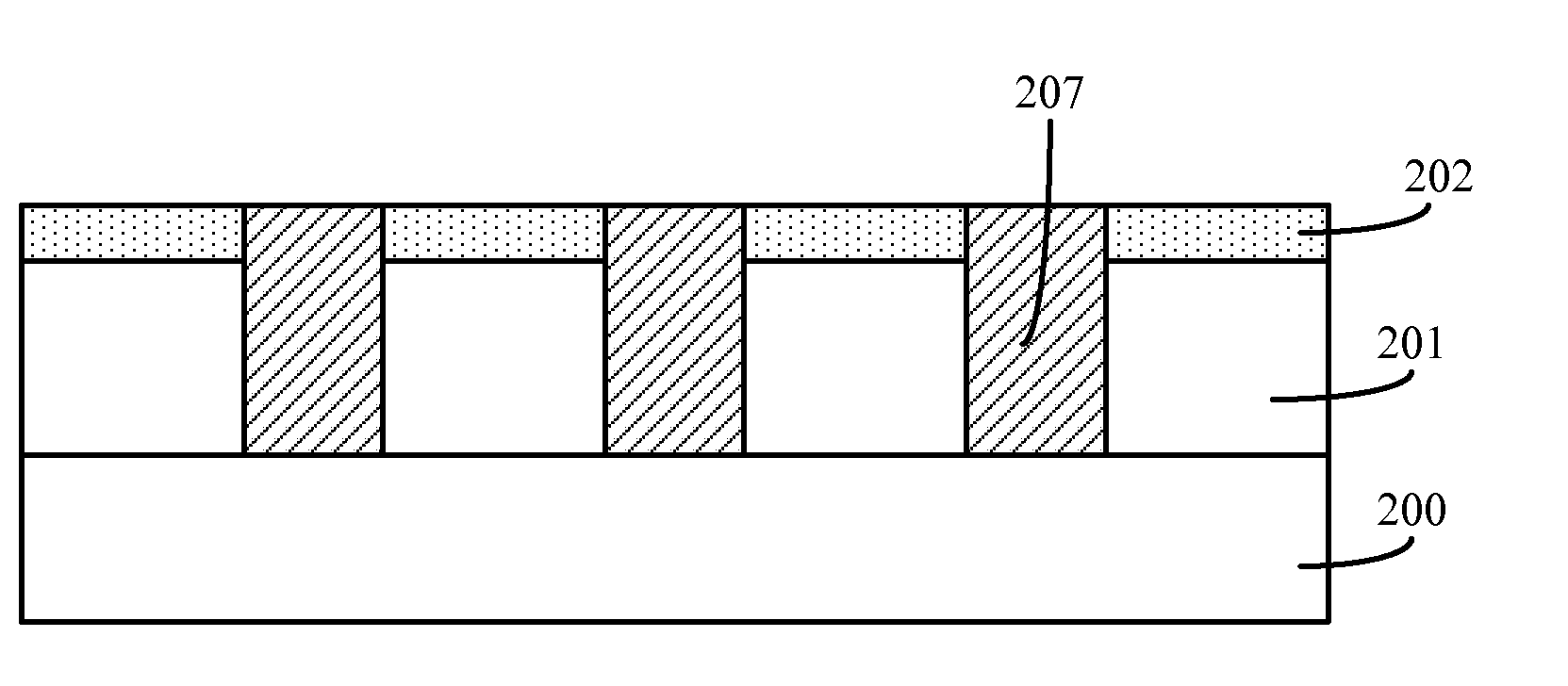
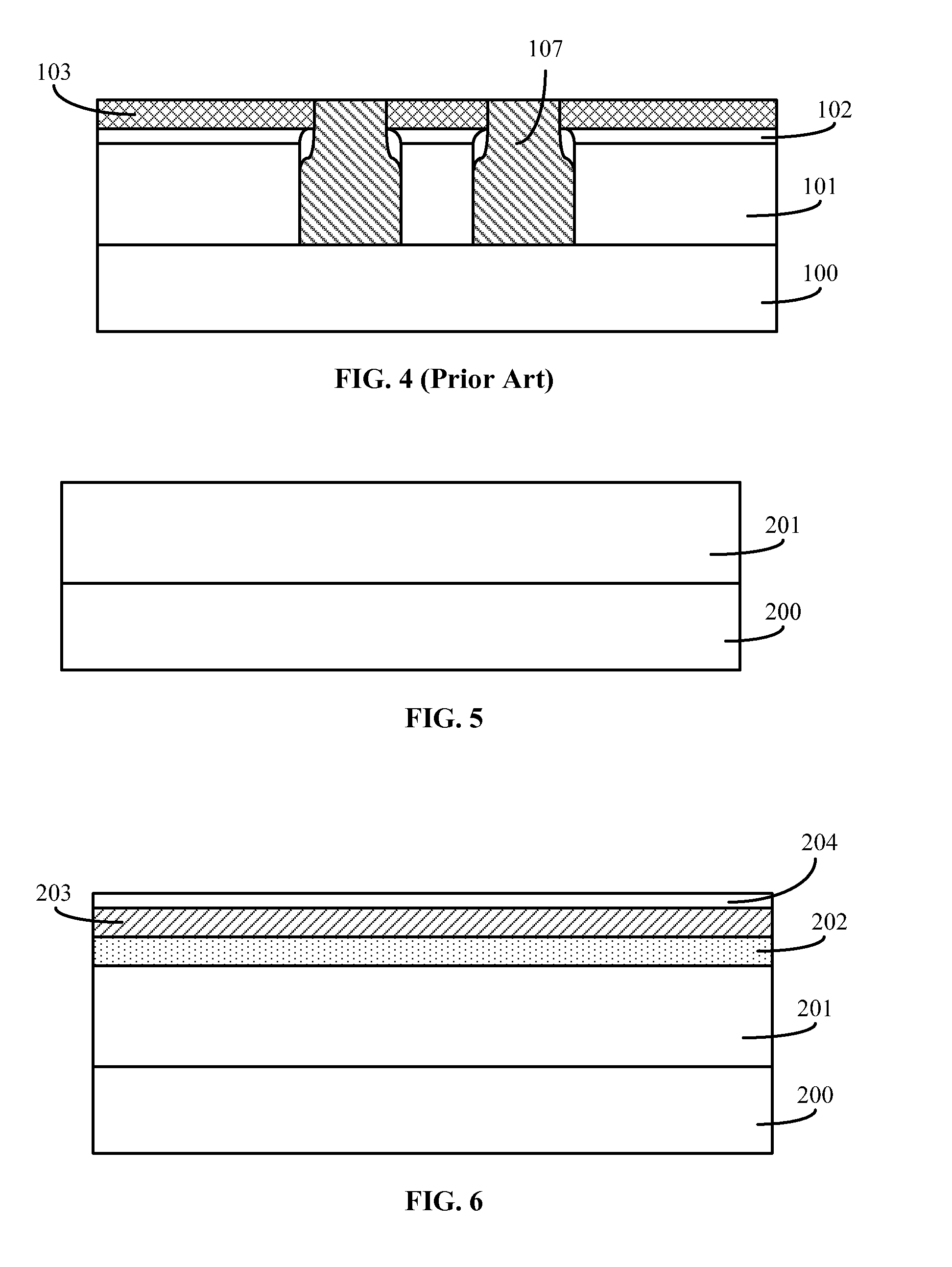
[0016]Reference will now be made in detail to exemplary embodiments of the invention, which are illustrated in the accompanying drawings. Wherever possible, the same reference numbers will be used throughout the drawings to refer to the same or like parts.

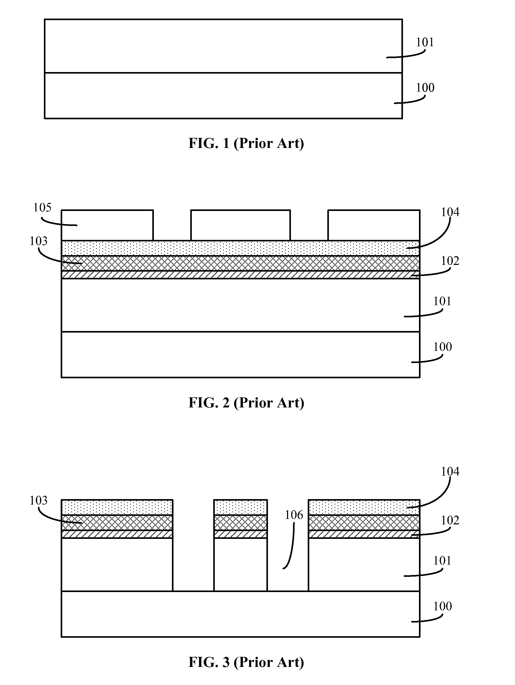
[0017]Referring to FIGS. 3-4, after forming the opening 106, a wet chemical cleaning process may be needed. Commonly used chemicals of the wet chemical cleaning process may include diluted hydrogen fluoride (HF). An etching rate of the hard mask layer 103 under an HF etching process may be slower than an etching rate of the buffer layer 102 under the HF etching process. Thus, after the wet chemical cleaning process, an undercut may be formed under the hard mask layer 103. That is, a sidewall of the etched hard mask layer 103 may protrude from a sidewall of the etched buffer layer 102. For example, when a diluted HF solution with a water to HF ratio of 200:1 is used to perform the wet chemical cleaning process, a distance between th...


PUM


Abstract

A method is provided for fabricating a semiconductor structure. The method includes providing a substrate; and forming a to-be-etched layer made of porous low dielectric constant material on one surface of the semiconductor substrate. The method also includes forming a first hard mask layer made of nitrogen-doped silicon oxycarbide (SiOC(N)) on the to-be-etched layer; and etching the first hard mask layer to have patterns corresponding to positions of subsequently formed openings. Further, the method includes forming the plurality of openings without substantial undercut between the to-be-etched layer and the first hard mask layer in the to-be-etched layer using the first hard mask layer as an etching mask; and forming a conductive structure in each of the openings.

Description

CROSS-REFERENCES TO RELATED APPLICATIONS[0001]This application claims the priority of Chinese patent application No. 201310315154.5, filed on Jul. 24, 2013, the entirety of which is incorporated herein by reference.FIELD OF THE INVENTION[0002]The present invention generally relates to the field of semiconductor manufacturing technology and, more particularly, relates to semiconductor structures and fabrication techniques thereof.BACKGROUND[0003]With the development on the integrated circuit (IC) technology, the integration level of semiconductor devices has been continuously improved, which causes the number of conductive structures in a circuit to significantly increase; and the distances between the conductive structures to decrease. Thus, a resistive capacitive delay (RC delay) effect caused by parasitic capacitances and parasitic resistances becomes more severe. In order to reduce the RC delay effect caused by the parasitic capacitances and the parasitic resistances, low dielect...

Claims


Application Information

Patent Timeline
IPC IPC(8): H01L21/768H01L23/522
CPCH01L21/76802H01L23/5226H01L21/76843H01L23/5329H01L23/53295H01L2924/0002H01L2924/00H01L21/02063H01L21/02126H01L21/02211H01L21/02274H01L21/31144
Inventor ZHOU, MING
Owner SEMICON MFG INT (SHANGHAI) CORP
Features
  • R&D
  • Intellectual Property
  • Life Sciences
  • Materials
  • Tech Scout
  • Unparalleled Data Quality
  • Higher Quality Content
  • 60% Fewer Hallucinations
Learn More