Method for evaluating degree of crystal orientation in polycrystalline silicon, selection method for polycrystalline silicon rods, and production method for single-crystal silicon

a technology of polycrystalline silicon and crystal orientation, applied in the direction of silicon compounds, material analysis using wave/particle radiation, instruments, etc., can solve the problems of loss of crystal lines and generation of dislocation, and achieve the effect of reducing local generation of partial melting residues and stable production of single-crystal silicon

Inactive Publication Date: 2015-02-19
SHIN ETSU CHEM IND CO LTD
View PDF1 Cites 4 Cited by
  • Summary
  • Abstract
  • Description
  • Claims
  • Application Information

AI Technical Summary

Benefits of technology

[0020]It is possible to suppress local generation of partial melting residue and contribute to stable production of single-crystal silicon by evaluating a degree of crystal orientation of polycrystalline silicon by the method according to the pr

Problems solved by technology

During this process, if unmelted polycrystalline silicon remains in the silicon melt, this unmelted polycrystalline piece floa

Method used


Image

  • Method for evaluating degree of crystal orientation in polycrystalline silicon, selection method for polycrystalline silicon rods, and production method for single-crystal silicon
  • Method for evaluating degree of crystal orientation in polycrystalline silicon, selection method for polycrystalline silicon rods, and production method for single-crystal silicon
  • Method for evaluating degree of crystal orientation in polycrystalline silicon, selection method for polycrystalline silicon rods, and production method for single-crystal silicon

Examples


examples

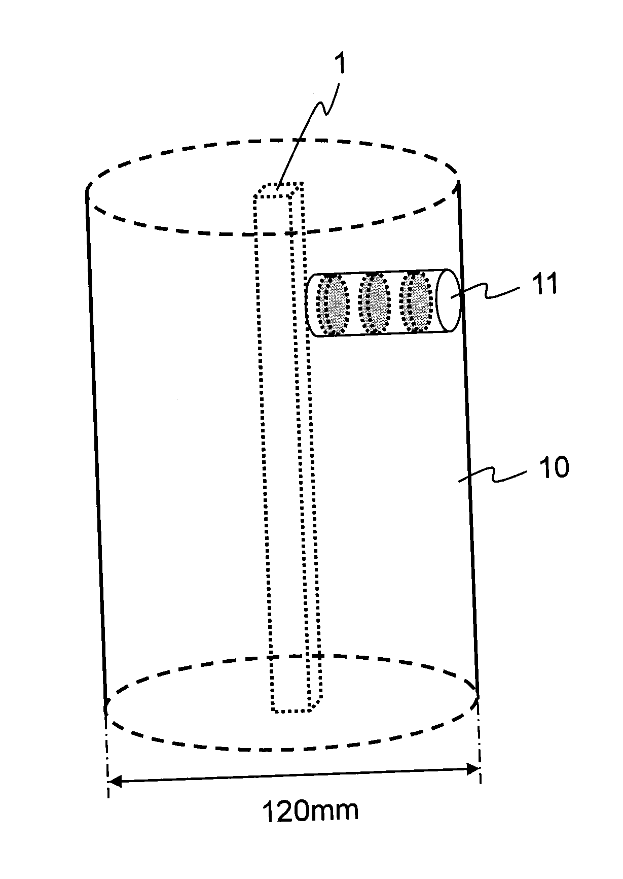
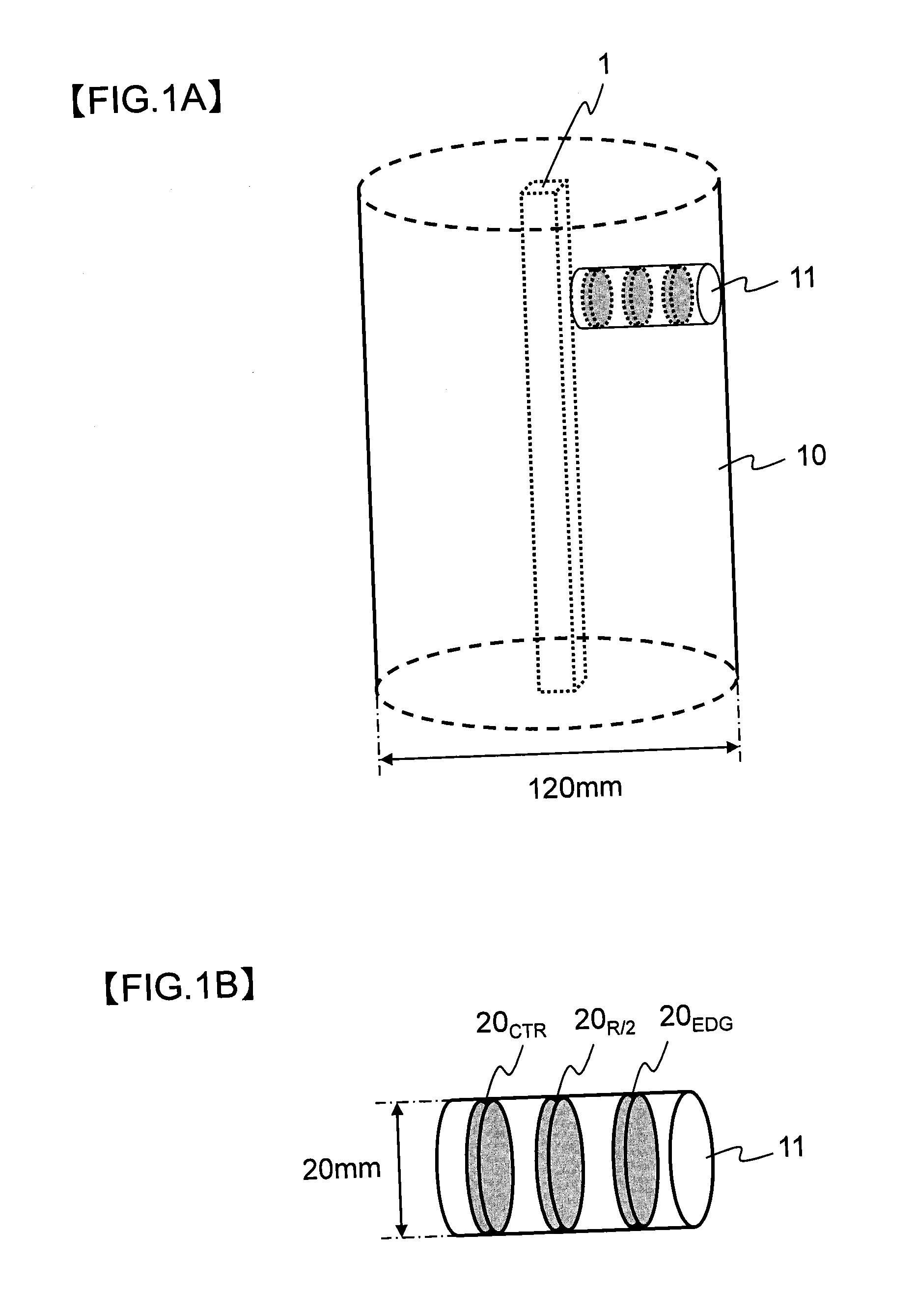
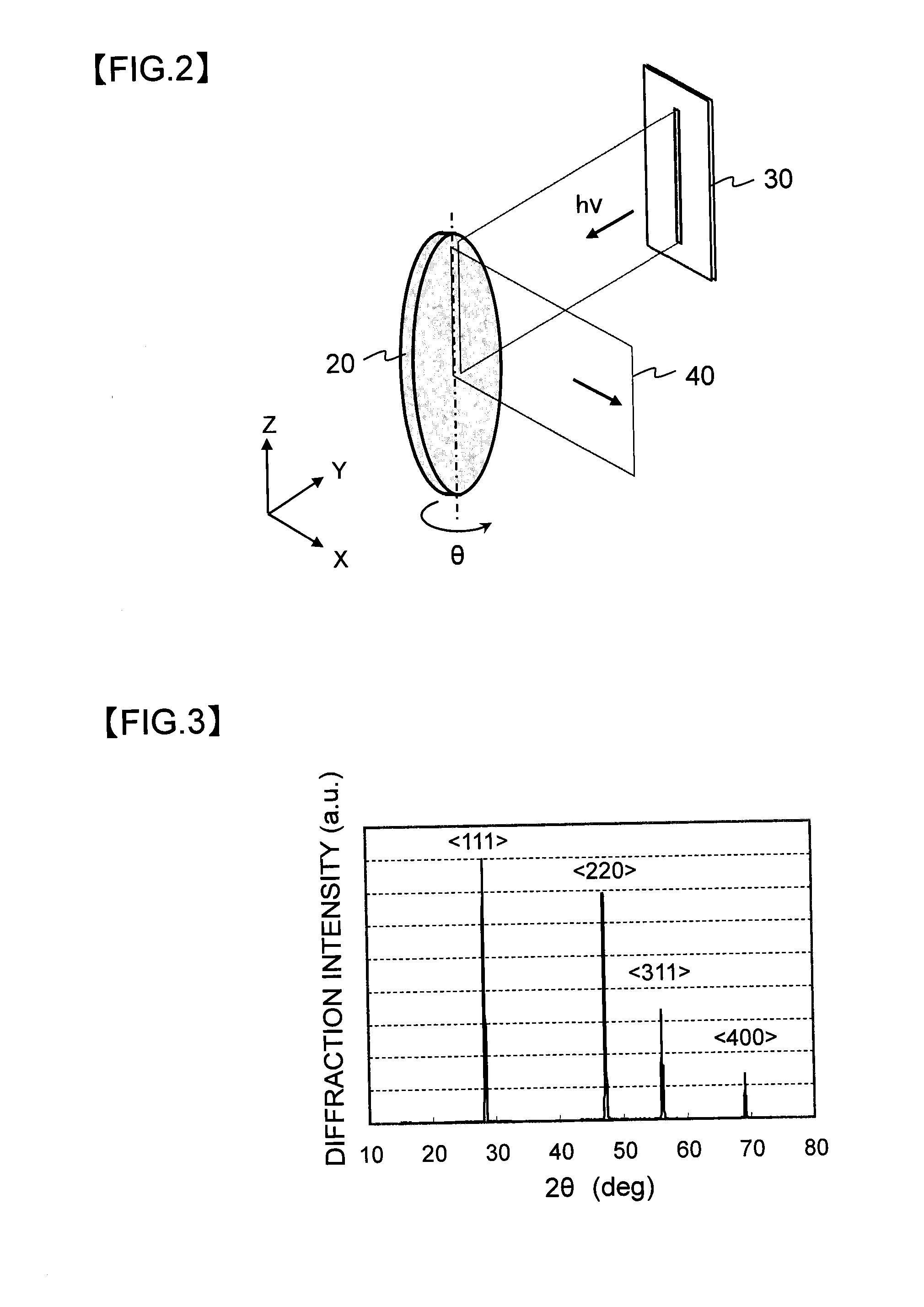
[0067]Four polycrystalline silicon rods grown under different deposition conditions were prepared. For each of these polycrystalline silicon rods (silicon rods A to D), roughly 2 mm thick plate-like samples (20CTR, 20EDG, and 20R / 2) were extracted from the three portions shown in FIGS. 1A and 1B, and by the measurement system shown in FIG. 6, a φ-scanning chart for the Miller index planes and was obtained. The diameter of the plate-like sample 20 was approximately 20 mm.

[0068]Table 1 summarizes, for each plate-like sample obtained from these polycrystalline silicon rods, the number of peaks (converted into unit per area) and the maximum value (maximum grain size) of the inhomogeneous crystal grain size calculated from these peaks, as well as whether there was loss of crystal lines when a single-crystal silicon rod was grown by the FZ method using the polycrystalline silicon rod.

TABLE 1Number of peaksMaximum grainLoss ofSiliconPlate-like(cm2)size (mm)crystalrodsamplelineA20CTR00——W...


PUM

PropertyMeasurementUnit
Grain sizeaaaaaaaaaa
Lengthaaaaaaaaaa
Ratioaaaaaaaaaa

Abstract

When a plate-like sample 20 extracted from a polycrystalline rod is evaluated, peaks can appear in a φ-scanning chart. The smaller the number of such peaks, and the narrower the half-value width of the peak, the more suitable the polycrystalline silicon rod is as a raw material for producing single-crystal silicon. It is preferable that the number of peaks in the φ-scanning chart is, for both the Miller index planes <111> and <220>, equal to or smaller than 24/cm2 when converted into unit per area of the plate-like sample. It is also preferable that the value obtained by multiplying the peak half-value width by δL=21/2πR0/360, where R0 is the radius of the sample, is defined as an inhomogeneous crystal grain size, and that a polycrystalline silicon rod of which all the inhomogeneous crystal grain sizes are smaller than 0.5 mm is selected as a raw material for producing single-crystal silicon.

Description

TECHNICAL FIELD[0001]The present invention relates to a method for evaluating a degree of crystal orientation of polycrystalline silicon, and a selection method, using this evaluation method, of a polycrystalline silicon rod which is used as a raw material for producing single-crystal silicon. More particularly, the present invention relates to a technology for selecting a non-oriented polycrystalline silicon rod which is suitable for stable production of single-crystal silicon.BACKGROUND ART[0002]Crystals of monocrystalline silicon which is essential for production of semiconductor devices, etc. are grown by a method such as the CZ method or the FZ method, and a polycrystalline silicon rod or a polycrystalline silicon ingot is used as the raw material. Such a polycrystalline silicon material is in most cases produced by the Siemens method (see Patent Literature 1). The Siemens method is a method involving bringing a source gas of silane such as trichlorosilane or mono-silane into c...

Claims


Application Information

Patent Timeline
IPC IPC(8): C30B13/34C01B33/02C23C16/24G01N23/207C30B29/06C30B25/02
CPCC30B13/34C30B29/06C30B25/02C01P2002/60G01N23/207C01B33/02C01P2002/74C23C16/24C30B35/007C30B13/00C30B15/00
Inventor MIYAO, SHUICHIOKADA, JUNICHINETSU, SHIGEYOSHI
Owner SHIN ETSU CHEM IND CO LTD
Why Eureka
Try Eureka