Method of electrochemically preparing silicon film
a technology of electrochemical preparation and silicon film, which is applied in the direction of liquid/solution decomposition chemical coating, sustainable manufacturing/processing, final product manufacturing, etc., can solve the problems of high cost, high energy consumption of conventional techniques, and large equipment requirements of multiple manufacturing processes, so as to reduce the production cost of semiconductors or solar cells, the effect of reducing energy consumption and being easy to prepar
- Summary
- Abstract
- Description
- Claims
- Application Information
AI Technical Summary
Benefits of technology
Problems solved by technology
Method used
Image

Examples
example 1
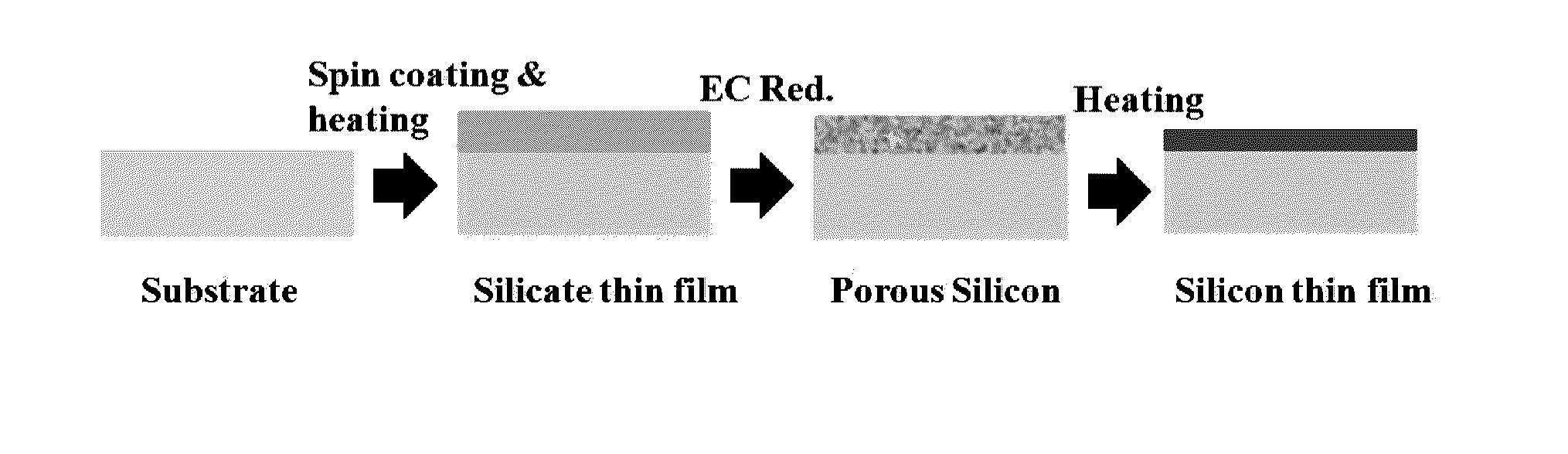
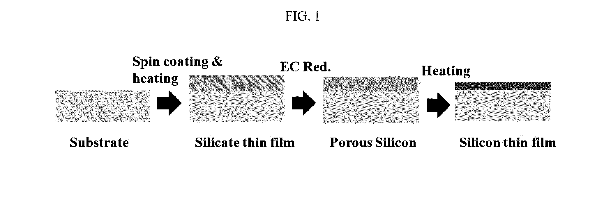
Preparation of Silicon Thin Film
[0092]1-1. Preparation of Silica Thin Film
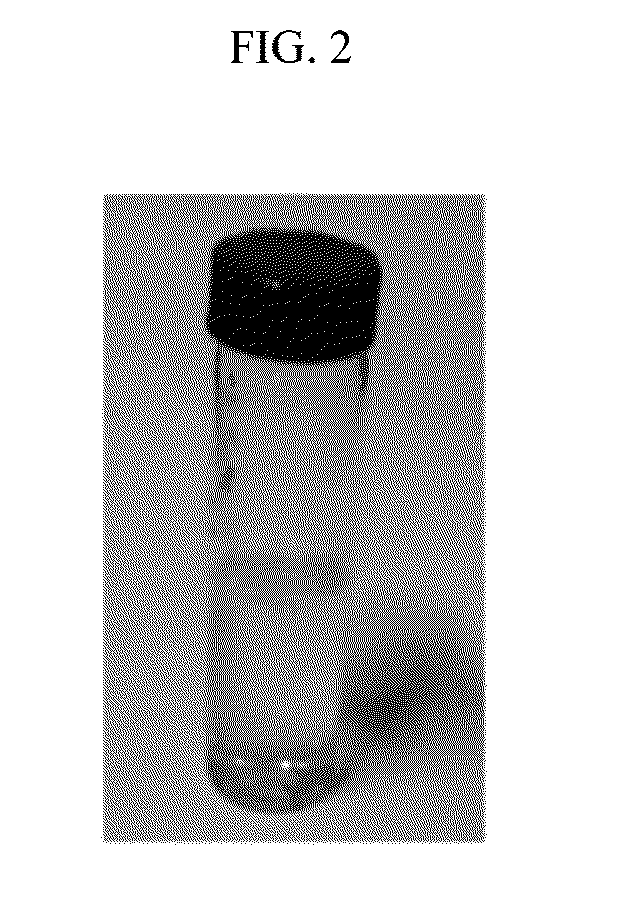
[0093]900 mg of silica powder was dissolved into 18 ml of a sodium hydroxide solvent, and kept for two days until the silica was completely dissolved, thereby preparing a spin coating solution (see FIG. 2).
[0094]A tungsten substrate was attached to a spin coater, and the spin coating solution was dropped on the tungsten substrate using a pipette while rotating the tungsten substrate at a rate of 500 to 10,000 rpm to form a silica thin film on the tungsten substrate. Thereafter, the coated silica thin film was dried and then sintered by heating at 130° C. for an hour.
[0095]In this case, it was confirmed under an electron microscope that the thickness of the silica thin film was in proportion to the concentration of silica dissolved in the spin coating solution, and was in inverse proportion to the rotation speed of the spin coater (see FIG. 3).
[0096]1-2. Electrochemical Reduction of Silica Thin Film
[0097]To pro...
example 2
Preparation of Carbon-Added Silicon Thin Film
[0103]900 mg of silica powder, and 0% by weight, 0.25% by weight and 0.5% by weight of potassium carbonate were separately added to three vials containing 18 ml sodium hydroxide solvent, and kept for two days until the silica and potassium carbonate were completely dissolved, thereby preparing a spin coating solution.
[0104]A tungsten substrate was attached to a spin coater, and the spin coating solution was dropped on the tungsten substrate using a pipette while rotating the tungsten substrate at a rate of 500 to 10,000 rpm to form a silica thin film on the tungsten substrate. Thereafter, the coated silica thin film was dried and then sintered by heating at 130° C. for an hour.
[0105]To produce a porous silicon thin film by electrochemically reducing the silica thin film prepared with spin coating and sintering methods, an electrochemical cell was set up.
[0106]The electrochemical cell was composed of the LiCl—KCl high-temperature molten sa...
example 3
Silicon Doping
[0111]First of all, 900 mg of silica powder, and 0.05% by weight, 0.15% by weight and 0.45% by weight of potassium nitrate were separately added to three vials containing 18 ml sodium hydroxide solvent, and kept for two days until the silica and potassium nitrate were completely dissolved, thereby preparing a spin coating solution.
[0112]A tungsten substrate was attached to a spin coater, and the spin coating solution was dropped on the tungsten substrate using a pipette while rotating the tungsten substrate at a rate of 500 to 10,000 rpm to form a silica thin film, to which nitrate ions was added, on the tungsten substrate. Thereafter, the coated silica thin film was dried and then sintered by heating at 130° C. for an hour.
[0113]To produce a porous N-doped silicon thin film by electrochemically reducing the silica thin film prepared with spin coating and sintering methods, an electrochemical cell was set up.
[0114]The electrochemical cell was composed of the LiCl—KCl h...
PUM
| Property | Measurement | Unit |
|---|---|---|
| pressure | aaaaa | aaaaa |
| temperature | aaaaa | aaaaa |
| weight | aaaaa | aaaaa |
Abstract
Description
Claims
Application Information
 - R&D
- Intellectual Property
- Life Sciences
- Materials
- Tech Scout
- Unparalleled Data Quality
- Higher Quality Content
- 60% Fewer Hallucinations
Browse by: Latest US Patents, China's latest patents, Technical Efficacy Thesaurus, Application Domain, Technology Topic, Popular Technical Reports.
© 2025 PatSnap. All rights reserved.Legal|Privacy policy|Modern Slavery Act Transparency Statement|Sitemap|About US| Contact US: help@patsnap.com