Method of manufacturing semiconductor device and semiconductor device

Inactive Publication Date: 2015-03-05
CANON KK
View PDF12 Cites 2 Cited by
  • Summary
  • Abstract
  • Description
  • Claims
  • Application Information

AI Technical Summary

Benefits of technology

[0009]One embodiment of the present disclosure has been devised to solve the above-described problem, and an objective thereof is to enable decreasing an amount o

Problems solved by technology

Between such films and silicon oxide, which is generally used as an interlayer insulating film, an interface stress is relatively large, w

Method used


Image

  • Method of manufacturing semiconductor device and semiconductor device
  • Method of manufacturing semiconductor device and semiconductor device
  • Method of manufacturing semiconductor device and semiconductor device

Examples


Example

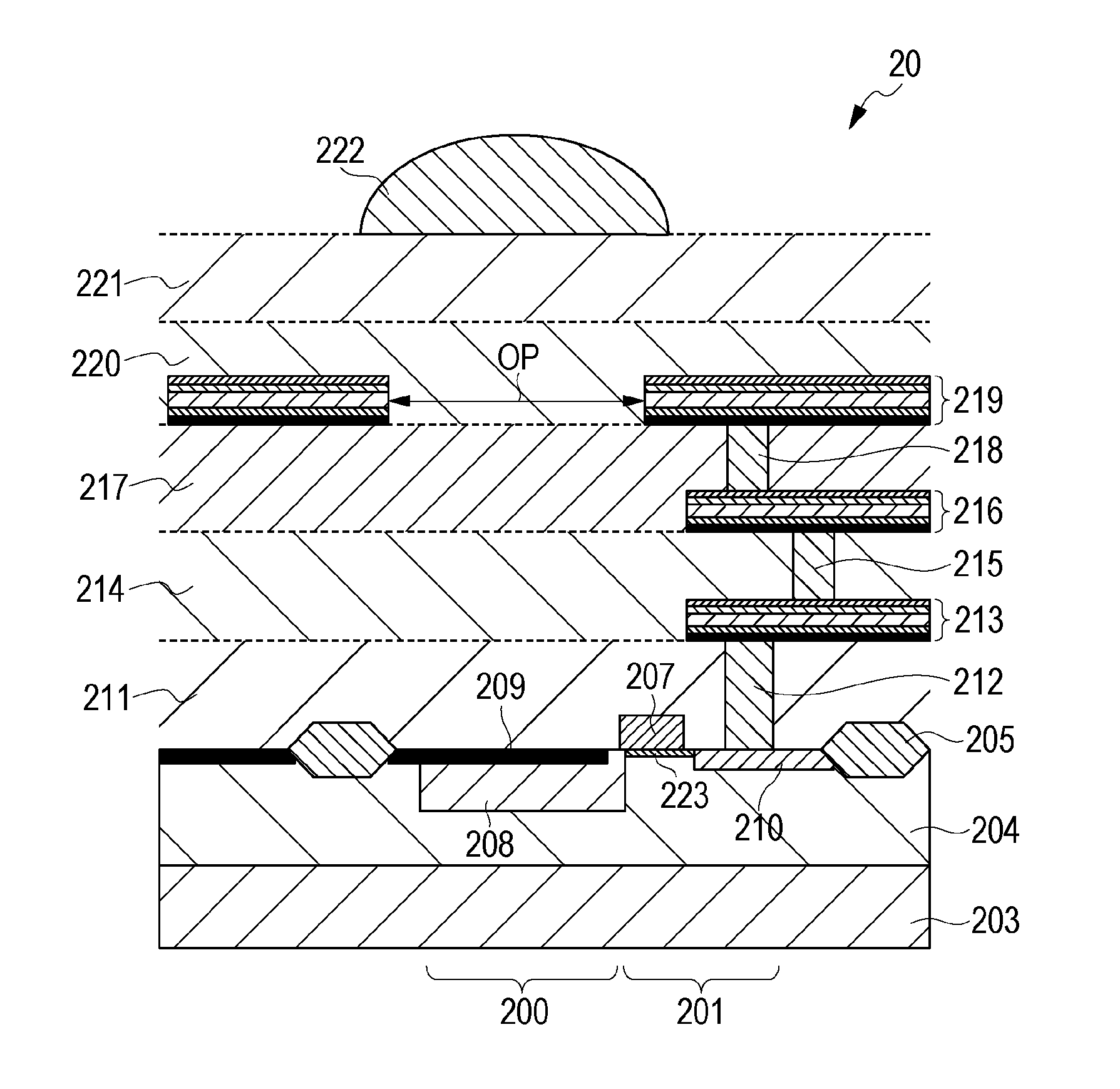
[0018]A first embodiment described herein is described by using FIG. 1. FIG. 1 is a semiconductor device in which wiring according to one embodiment of the present disclosure is used. In a description, an image pickup device is used as one example of the semiconductor device. FIG. 1 is a view schematically illustrating a section of the image pickup device. Note that a well-known or publicly known technique in the particular art is to be applied to a part not illustrated or described herein. Embodiments described hereinafter are exemplary embodiments of the present disclosure, and embodiments are not to be limited to these. The embodiment below is described by taking an example of a case where an electron is used as a signal carrier. In a case where a hole is used as the signal carrier, all of conductivity types may be reversed for each semiconductor area and an impurity region.

[0019]In FIG. 1, an image pickup device is described by taking a CMOS area sensor as an example. The CMOS a...

Example

Second Embodiment

[0054]Next, one example of an image pickup system using an image pickup device is illustrated in FIG. 4. An image pickup system 90, as illustrated in FIG. 4, is provided mainly with an optical system, the image pickup device 20 described in the first embodiment, and a signal processing unit. The optical system is mainly provided with a shutter 91, a lens 92, and a diaphragm 93. The signal processing unit is mainly provided with a picked-up signal processing circuit 95, an A / D converter 96, an imaging signal processing unit 97, a memory unit 87, an external I / F unit 89, a timing generation unit 98, an overall control / calculation unit 99, a recording medium 88, and a recording medium control I / F unit 94. Note that the signal processing unit may not be provided with the recording medium 88. The shutter 91 is provided before the lens 92 on an optical path and controls exposure. The lens 92 refracts light that has entered and forms an image of a subject on an image picku...


PUM


Abstract

A method of manufacturing a semiconductor device provided with an interlayer insulating film formed on a semiconductor substrate, and a plurality of wiring layers formed on the interlayer insulating film. The method includes forming of a first wiring layer closest to the semiconductor substrate among the plurality of wiring layers, and forming of an alloy of a titanium layer and a metal layer by heating treatment. The forming of the first wiring layer includes: forming of a titanium layer on an interlayer insulating film; forming of a metal layer containing a metal capable of forming an alloy with titanium in the titanium layer; forming of an orientation layer on the metal layer; and forming of an aluminum layer on the orientation layer.

Description

BACKGROUND[0001]1. Field of the Invention[0002]The present disclosure relates to a method of manufacturing a semiconductor device and the semiconductor device.[0003]2. Description of the Related Art[0004]Various types of metal wiring are disposed on a semiconductor substrate for transferring a signal and controlling operation of a device. The wiring is formed in an interlayer insulating film formed on the semiconductor substrate, and aluminum is widely used as a main material thereof.[0005]Then, in order to improve an electromigration resistance (hereinafter, also referred to as EM) feature in a case where the aluminum is used, there is used the wiring in which titanium, titanium nitride, and aluminum are laminated from lower to upper layers in order.[0006]By the way, in manufacturing of the semiconductor device, hydrogen processing (sintering) is performed, for example, to terminate a dangling bond in a semiconductor layer.[0007]In Japanese Patent Application Laid-Open No. 2010-153...

Claims


Application Information

Patent Timeline
IPC IPC(8): H01L21/48H01L31/18
CPCH01L31/18H01L21/4846H01L23/5226H01L23/5283H01L27/14636H01L27/14643H01L27/14689H01L2924/0002H01L2924/00
Inventor SUZUKI, YUKINOBU
Owner CANON KK
Why Eureka
Try Eureka