Active organic electroluminescence device back panel and manufacturing method thereof

a back panel and active organic technology, applied in the field of flat display, can solve the problems of increasing operating voltage, difficult to define the grey level of an active organic electroluminescence device, and disadvantageous curves in the sub-threshold zone, etc., and achieves low operating voltage, simple structure, and easy definition

Active Publication Date: 2015-03-12
SHENZHEN CHINA STAR OPTOELECTRONICS TECH CO LTD
View PDF2 Cites 16 Cited by
  • Summary
  • Abstract
  • Description
  • Claims
  • Application Information

AI Technical Summary

Benefits of technology

[0011]An object of the present invention is to provide an active organic electroluminescence device back panel, which has a sim

Problems solved by technology

Generally, curves that have very high slopes in the sub-threshold zone are disadvantageous for input control of a control voltage that reflects grey level variation.
Thus, when the sub-threshold swing of a thin-film transistor is relatively small, it would be difficult to define the grey levels of an organic electroluminescence device.
On the other hand, if the thickness of the gate insulation layer is increased to increase the sub-thr

Method used


Image

  • Active organic electroluminescence device back panel and manufacturing method thereof
  • Active organic electroluminescence device back panel and manufacturing method thereof
  • Active organic electroluminescence device back panel and manufacturing method thereof

Examples


Embodiment Construction

[0044]To further expound the technical solution adopted in the present invention and the advantages thereof, a detailed description is given to a preferred embodiment of the present invention and the attached drawings.

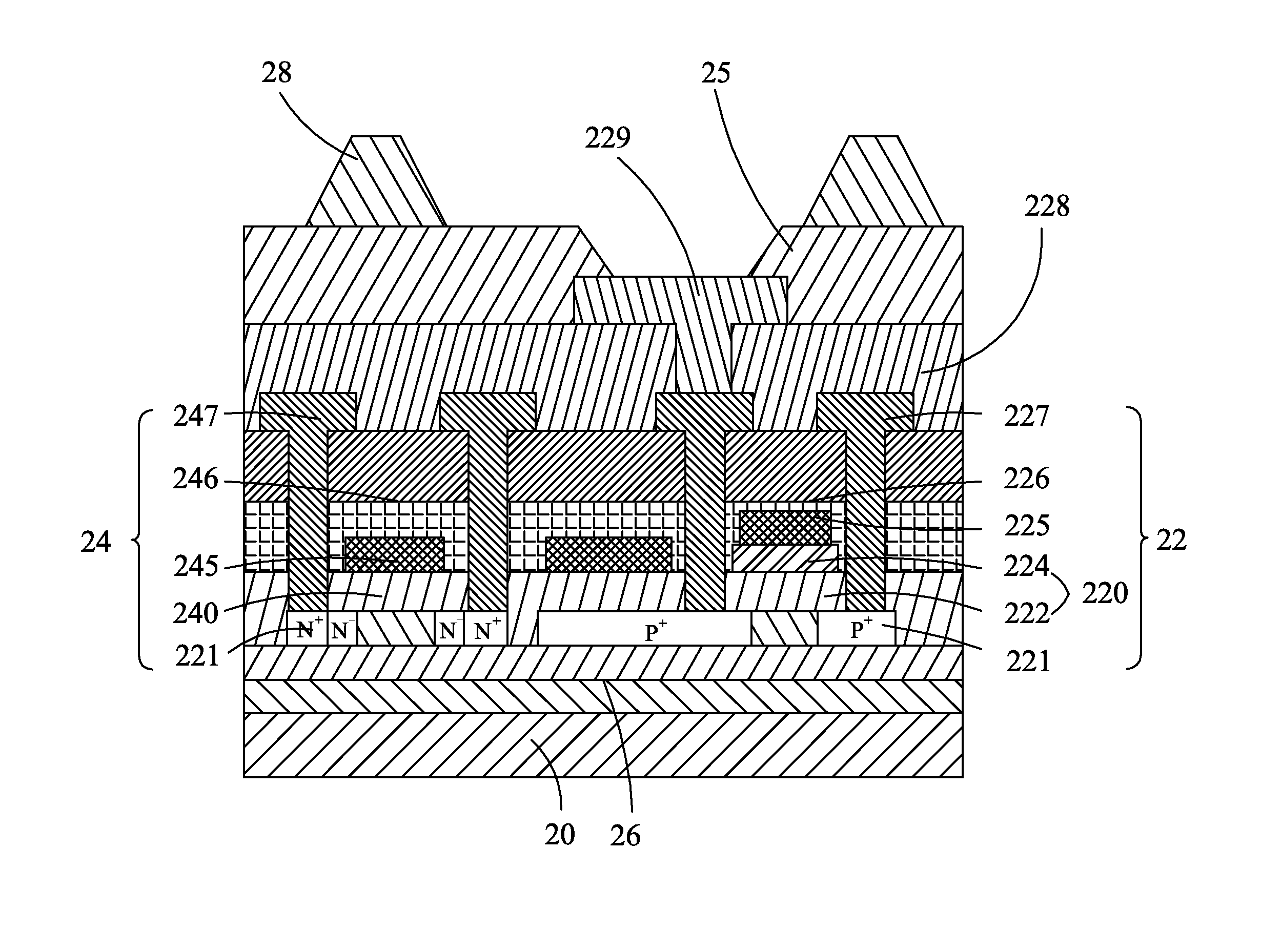
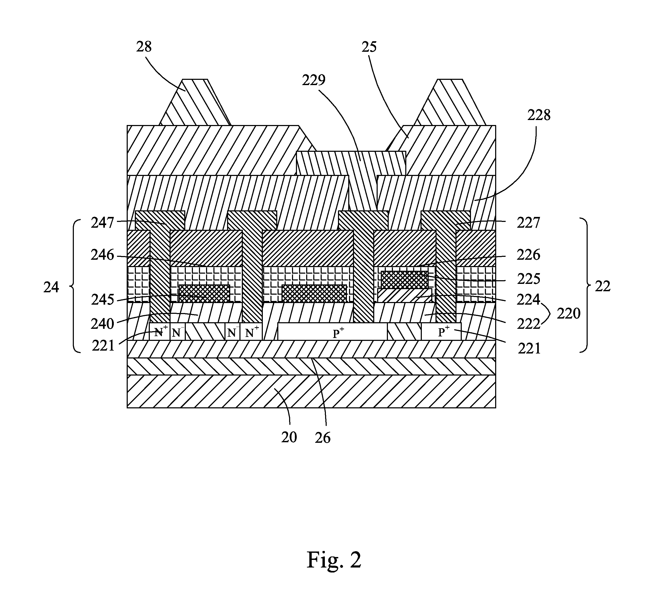
[0045]Referring to FIG. 2, the present invention provides an active organic electroluminescence device back panel, which comprises: a substrate 20, a plurality of active thin-film transistor (TFT) pixel arrays formed on the substrate 20, and organic planarization layers 228, organic electroluminescence electrodes 229, pixel definition layers 25, and support bodies 28 formed on the active TFT pixel arrays. Each of the active TFT pixel arrays comprises a driving TFT 22 and a switch TFT 24. The driving TFT 22 has a gate insulation layer 220 that has a thickness greater than a thickness of a gate insulation layer 240 of the switch TFT 24, whereby the driving TFT 22 has gate capacitance that is less than gate capacitance of the switch TFT 24 and thus, the driving TFT 22 has...


PUM


Abstract

The present invention provides an active organic electroluminescence device back panel and a manufacturing method thereof. The device back panel includes: a substrate (20), a plurality of active TFT pixel arrays formed on the substrate (20), and organic planarization layers (228), organic electroluminescence electrodes (229), pixel definition layers (25), and support bodies (28) formed on the active TFT pixel arrays. Each of the active TFT pixel arrays includes a driving TFT (22) and a switch TFT (24). The driving TFT (22) has a gate insulation layer (220) that has a thickness greater than a thickness of a gate insulation layer (240) of the switch TFT (24). Through thickening the gate insulation layer of the driving TFT, the gate capacitance of the driving TFT can be reduced and the sub-threshold swing of the driving TFT is increased to realize well definition of grey levels. Further, the thickness of the gate insulation layer of the switch TFT can be kept unchanged so that the sub-threshold swing of the switch TFT maintains relatively small so as to lower down the operating voltage and increase the circuit operation speed to thereby effectively improve the quality of the organic electroluminescence device.

Description

BACKGROUND OF THE INVENTION[0001]1. Field of the Invention[0002]The present invention relates to the field of flat displaying, and in particular to an active organic electroluminescence device back panel and a manufacturing method thereof.[0003]2. The Related Arts[0004]A flat display device has various advantages, such as thin device body, low power consumption, and being free of radiation, and is thus of wide applications. The flat display devices that are currently available include liquid crystal displays (LCDs) and organic electroluminescence devices (OELDs), which are also referred to as organic light emitting diodes (OLEDs).[0005]The known liquid crystal displays are generally backlighting liquid crystal displays, which include an enclosure, a liquid crystal display panel arranged in the enclosure, and a backlight module mounted inside the enclosure. The principle of operation of the liquid crystal display panel is that liquid crystal molecules are interposed between two paral...

Claims


Application Information

Patent Timeline
IPC IPC(8): H01L27/32H01L51/56
CPCH01L51/56H01L27/3262H01L27/1237H10K59/122H10K59/1213H10K59/00H10K71/00
Inventor HSU, YUANJUN
Owner SHENZHEN CHINA STAR OPTOELECTRONICS TECH CO LTD
Why Eureka
Try Eureka