
Thin film solar cell and method of fabricating the same
a technology solar cells, which is applied in the direction of sustainable manufacturing/processing, final product manufacturing, vacuum evaporation coating, etc., can solve the problems of low efficiency of thin film solar cells, high material cost of indium (in), and grain boundary defects, etc., to achieve excellent current-voltage characteristics, light conversion efficiency, and suppress grain boundary defects
- Summary
- Abstract
- Description
- Claims
- Application Information
AI Technical Summary
Benefits of technology
Problems solved by technology
Method used
Image

Examples
example 1
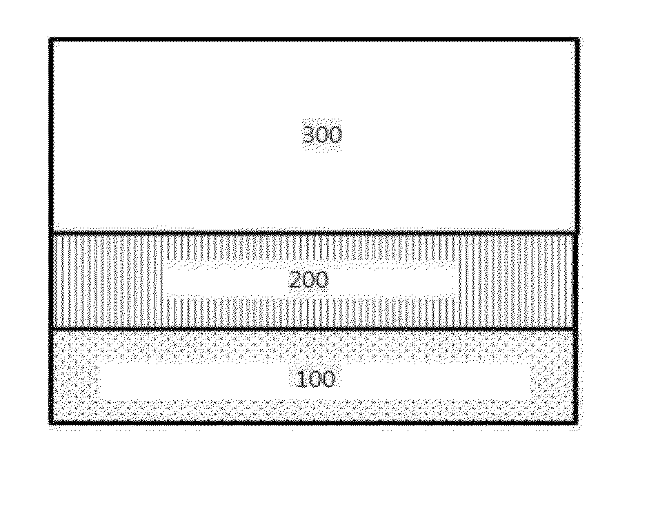
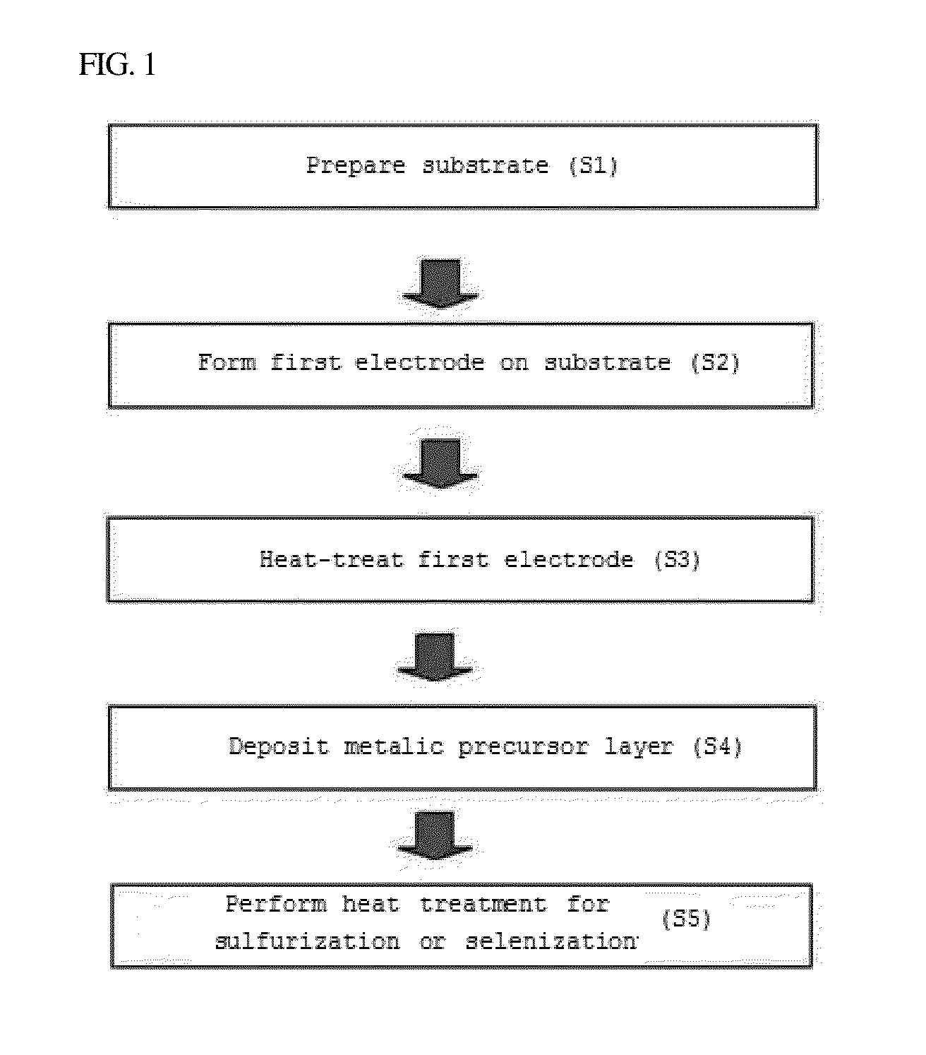
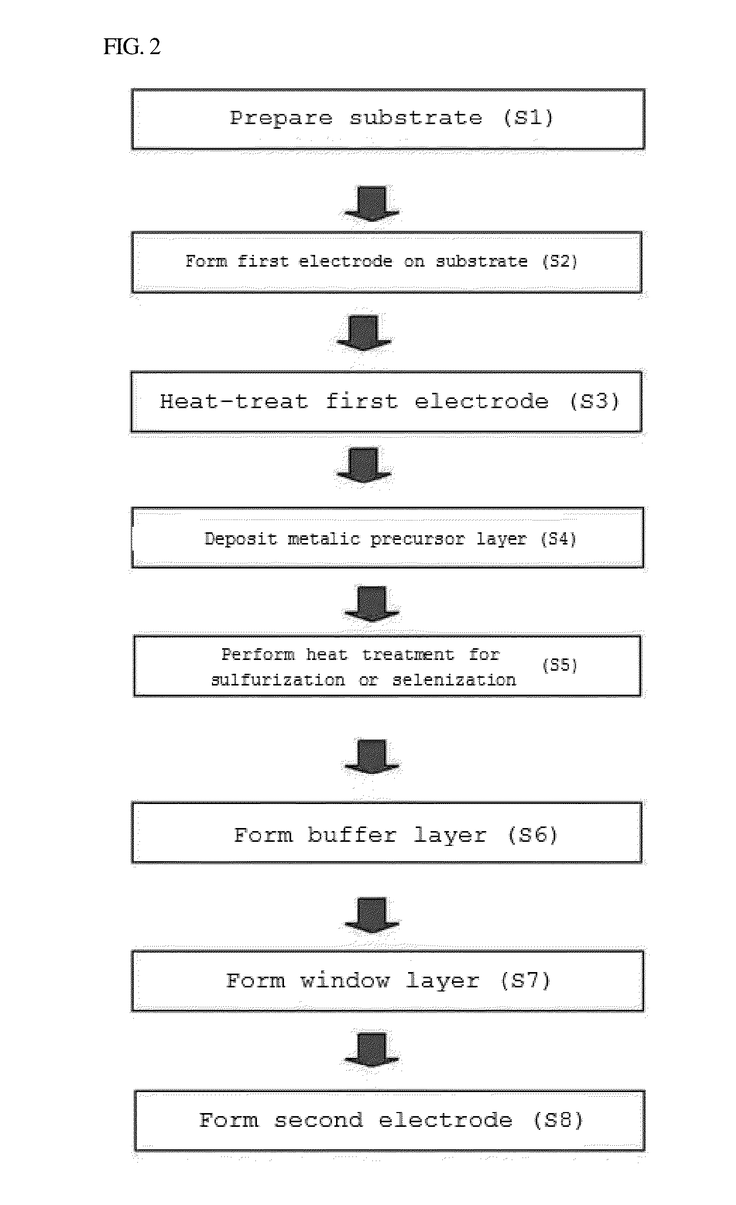
[0065]A soda lime glass substrate (100) was prepared, and a first electrode (200) of molybdenum (Mo) was deposited to have a thickness of about 0.5 μm on the substrate (100) through DC sputtering.
[0066]The first electrode was heat-treated at 400° C. for 10 minutes under nitrogen atmosphere.
example 2
[0067]A first electrode was formed by the same method as in example 1 except that the first electrode was heat-treated at 600° C.
manufacture examples 1 to 4
[0072]A CZT-based metallic precursor layer was formed by sputter-depositing a Zn precursor (301), a Sn precursor (302), and a Cu precursor (303) on each of the first electrodes (200) formed in examples 1 and 2 and comparative examples in the order shown in FIG. 5.
[0073]After that, the CZT-based metallic precursor layer was heat-treated according to a sulfurizing process. The heat treatment was conducted in a furnace including a first furnace and a second furnace. A sulfur (S) powder was heated at 300° C. in the first furnace, and the first electrode formed in example 1 was put in the second furnace, followed by a sulfurization treatment at a temperature of 600° C. As a result, as shown in FIG. 6, a CZTS-based light absorbing layer (300) was formed.
[0074]Then, a CdS buffer layer (400) of 60 nm, a ZnO window layer (500) of 400 nm, and an Al electrode (600) were formed on the CZTS-based light absorbing layer, thereby completing a CZTS-based thin film solar cell.
[0075](Photographing of ...
PUM
| Property | Measurement | Unit |
|---|---|---|
| thickness | aaaaa | aaaaa |
| thickness | aaaaa | aaaaa |
| thickness | aaaaa | aaaaa |
Abstract
Description
Claims
Application Information