

Semiconductor memory device and method for manufacturing the same
a memory device and semiconductor technology, applied in the direction of semiconductor devices, electrical devices, transistors, etc., can solve the problems of small gate coupling ratio between, affecting cell performance, difficult control, etc., and achieve the effect of improving performance, facilitating manufacturing and improving performan
- Summary
- Abstract
- Description
- Claims
- Application Information
AI Technical Summary
Benefits of technology
Problems solved by technology
Method used
Image

Examples
Embodiment Construction
[0014]In the following detailed description of the present invention, reference is made to the accompanying drawings which form a part hereof and is shown by way of illustration and specific embodiments in which the invention may be practiced. These embodiments are described in sufficient details to enable those skilled in the art to practice the invention. Other embodiments may be utilized and structural, logical, and electrical changes may be made without departing from the scope of the present invention. The following detailed description, therefore, is not to be taken in a limiting sense, and the scope of the present invention is defined by the appended claims.
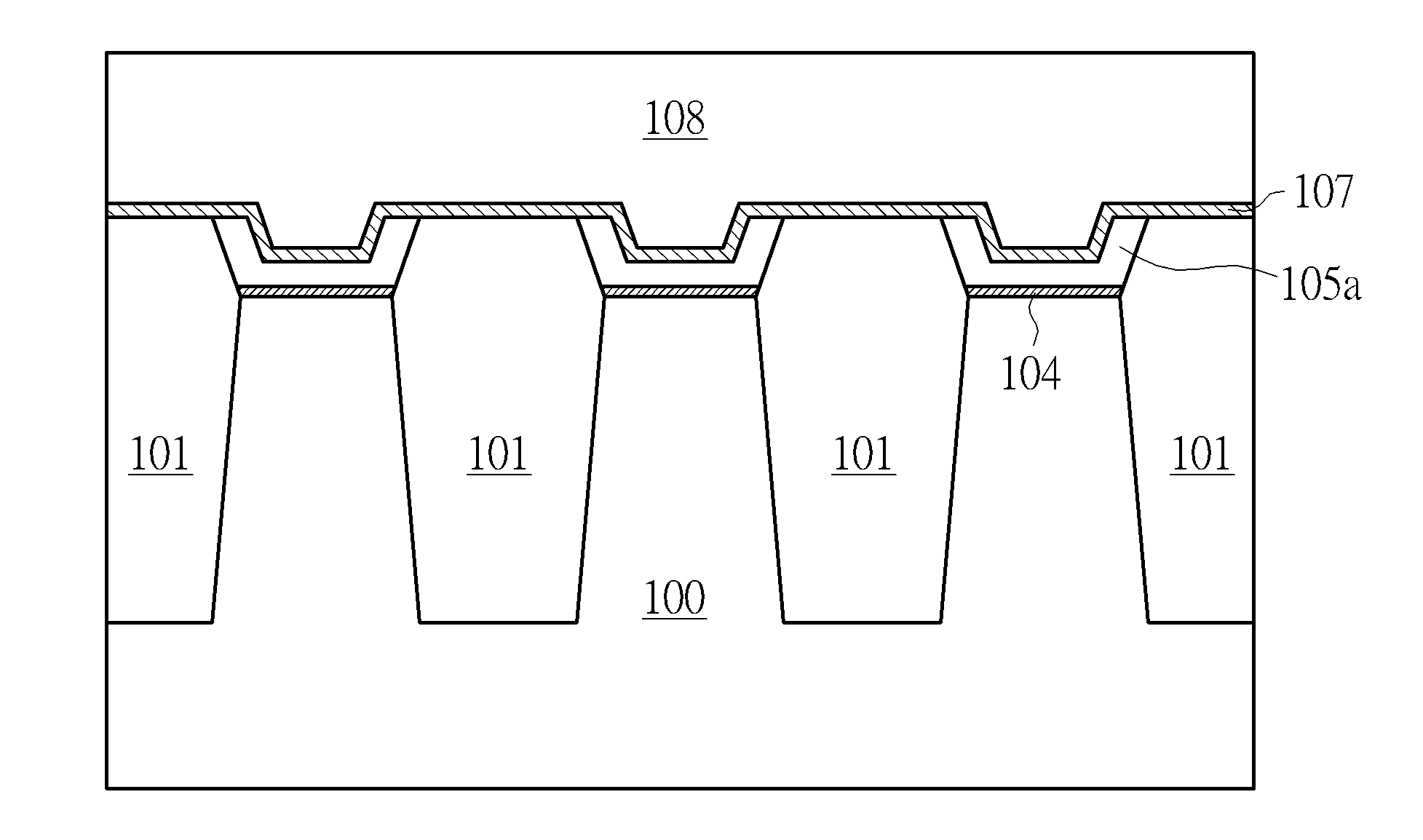
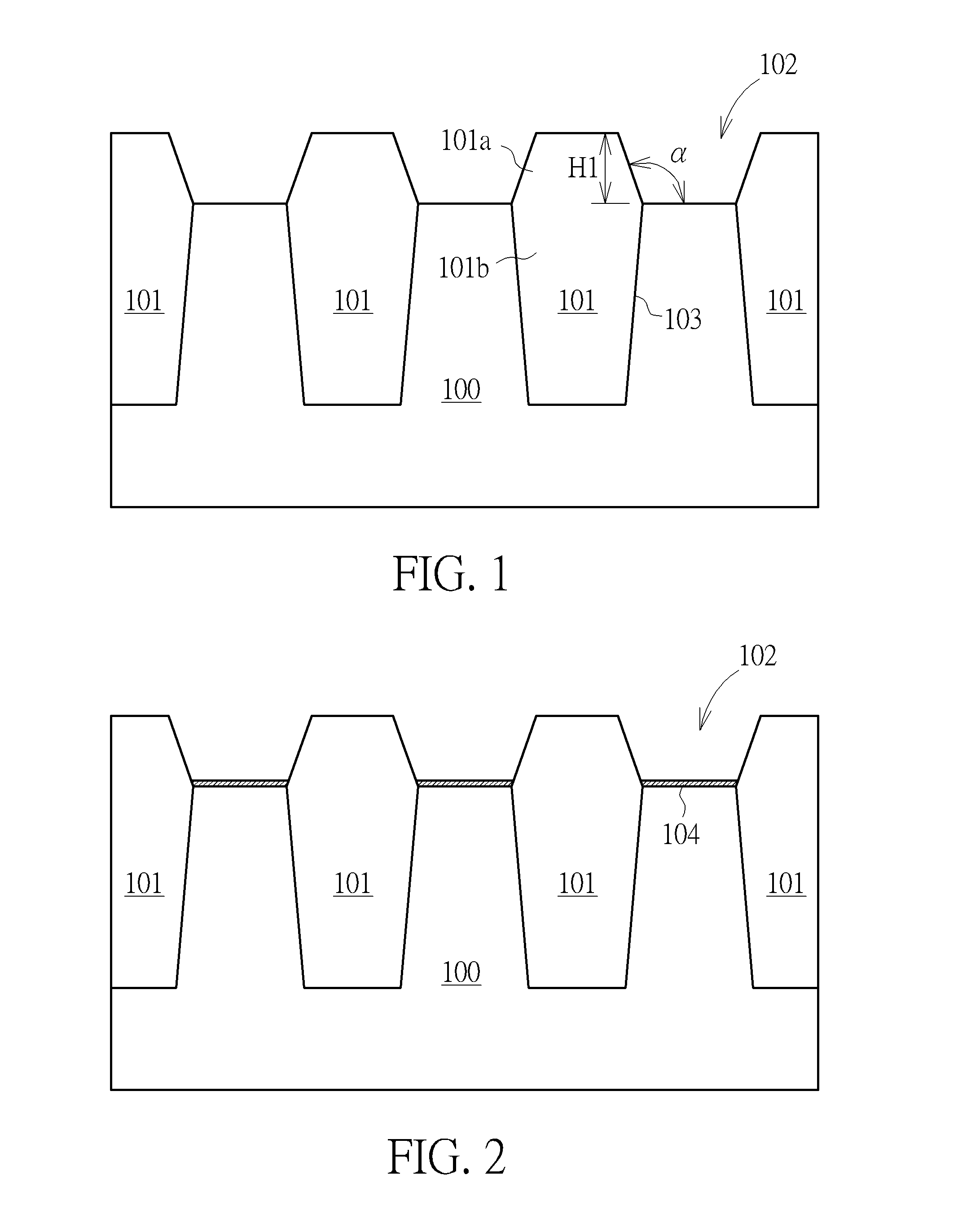
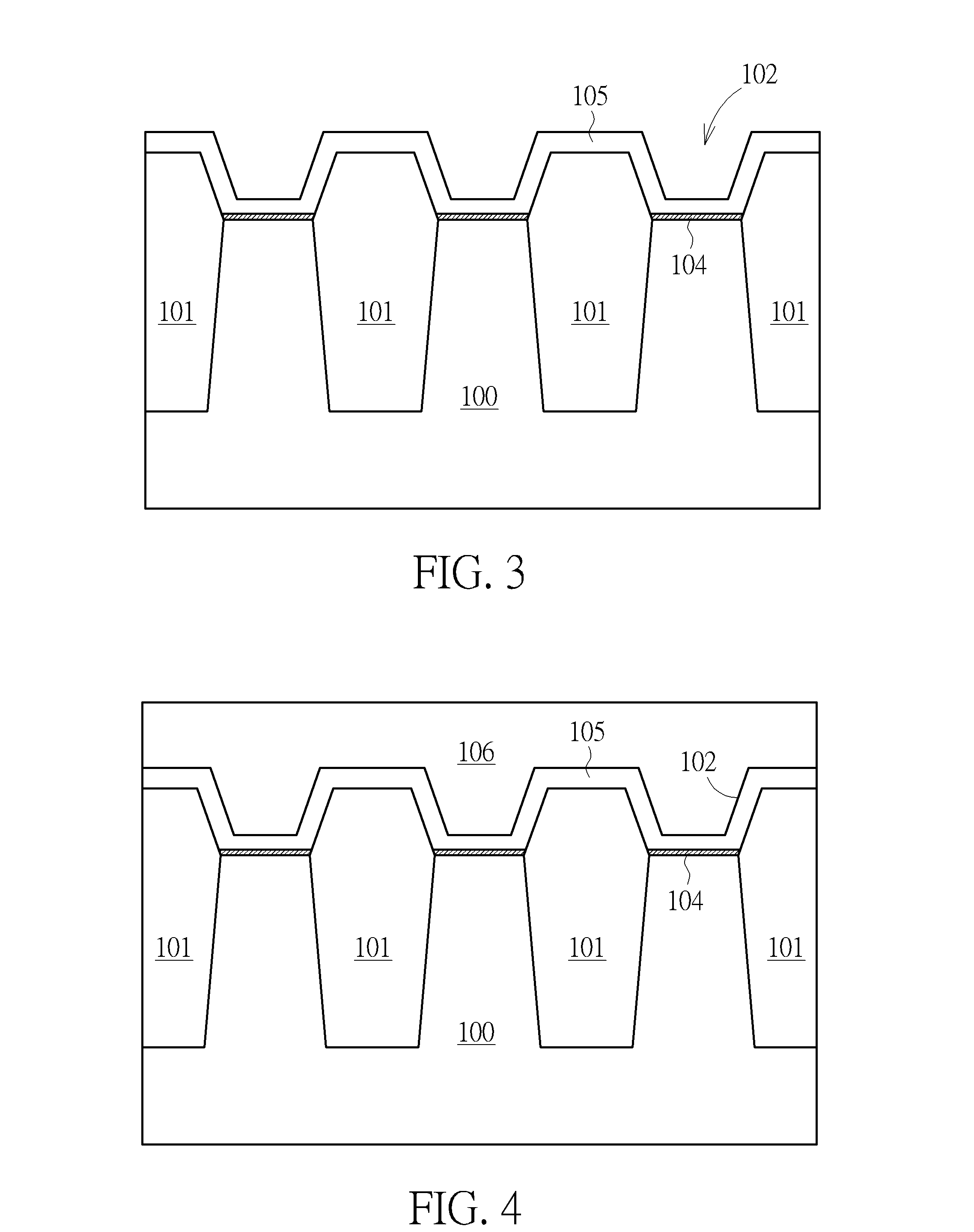
[0015]Please refer to FIGS. 1-7, which are cross-sectional views schematically depicting a process flow for manufacturing a semiconductor device in accordance with one embodiment of the present invention. First, as shown in FIG. 1, a semiconductor substrate 100 is provided to serve as a base for forming devices, components...
PUM
 Abstract
Description
Claims
Application Information