Dual gate fd-soi transistor

a transistor and gate technology, applied in the direction of transistors, semiconductor devices, electrical equipment, etc., can solve the problems of leaking current, device prone to drain battery, and device not ideal as integrated circuit construction,

Inactive Publication Date: 2015-05-14
STMICROELECTRONICS INT NV
View PDF10 Cites 12 Cited by
  • Summary
  • Abstract
  • Description
  • Claims
  • Application Information

AI Technical Summary

Problems solved by technology

Unfortunately, a transistor is not ideal as constructed in an integrated circuit and tends to leak current even when it is off.
Current that leaks through, or out of, the device tends to drain the battery that supplies power to the device.
However, as dimensions of silic

Method used


Image

  • Dual gate fd-soi transistor
  • Dual gate fd-soi transistor
  • Dual gate fd-soi transistor

Examples


Embodiment Construction

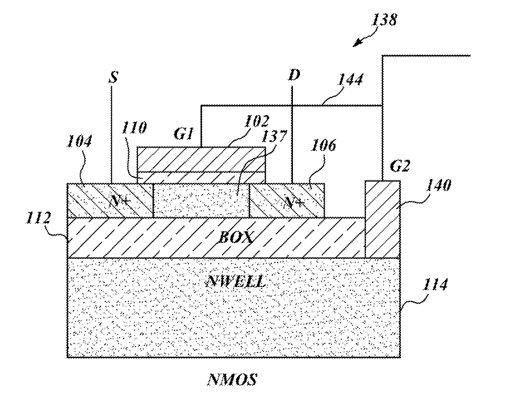
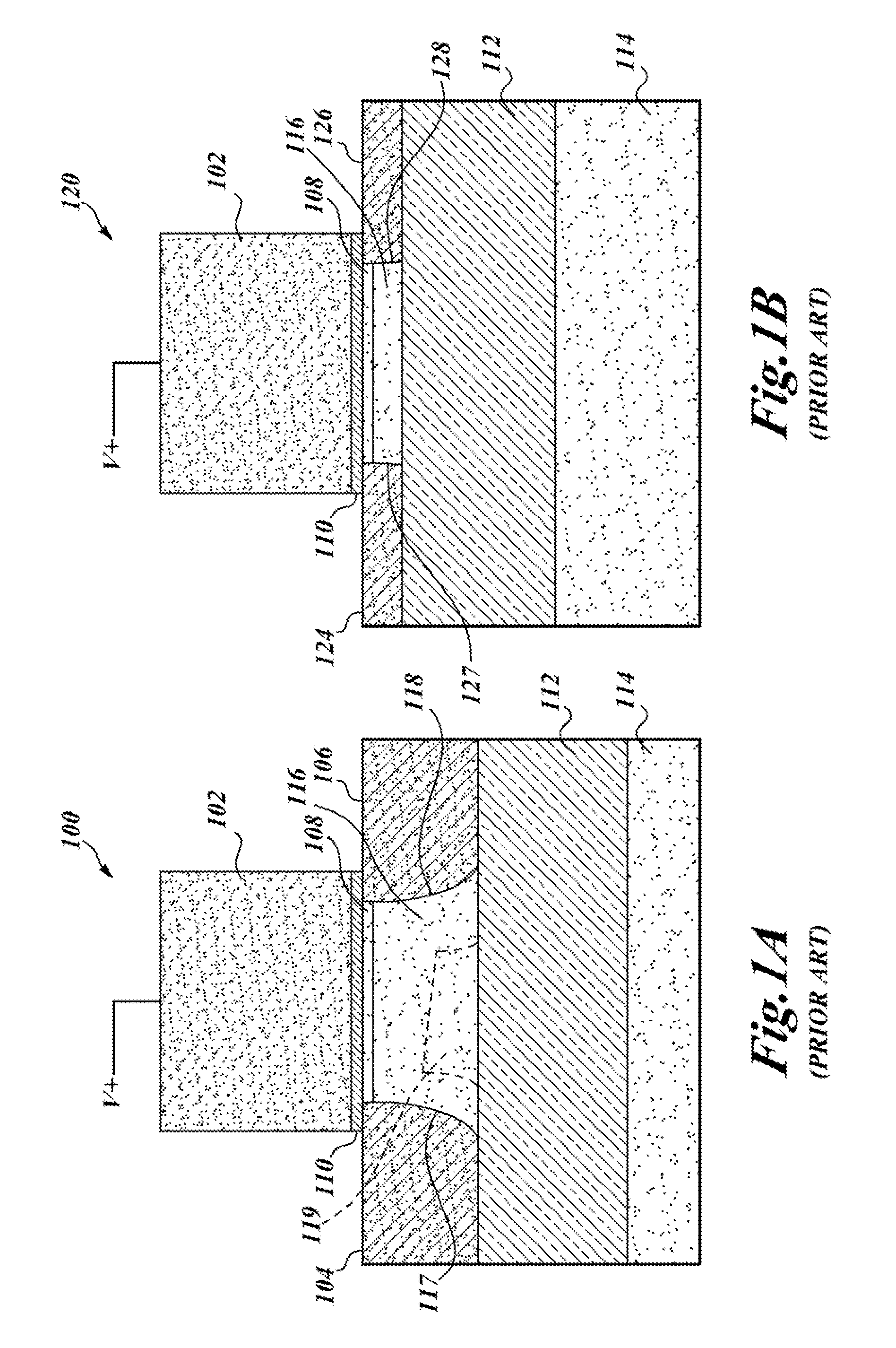
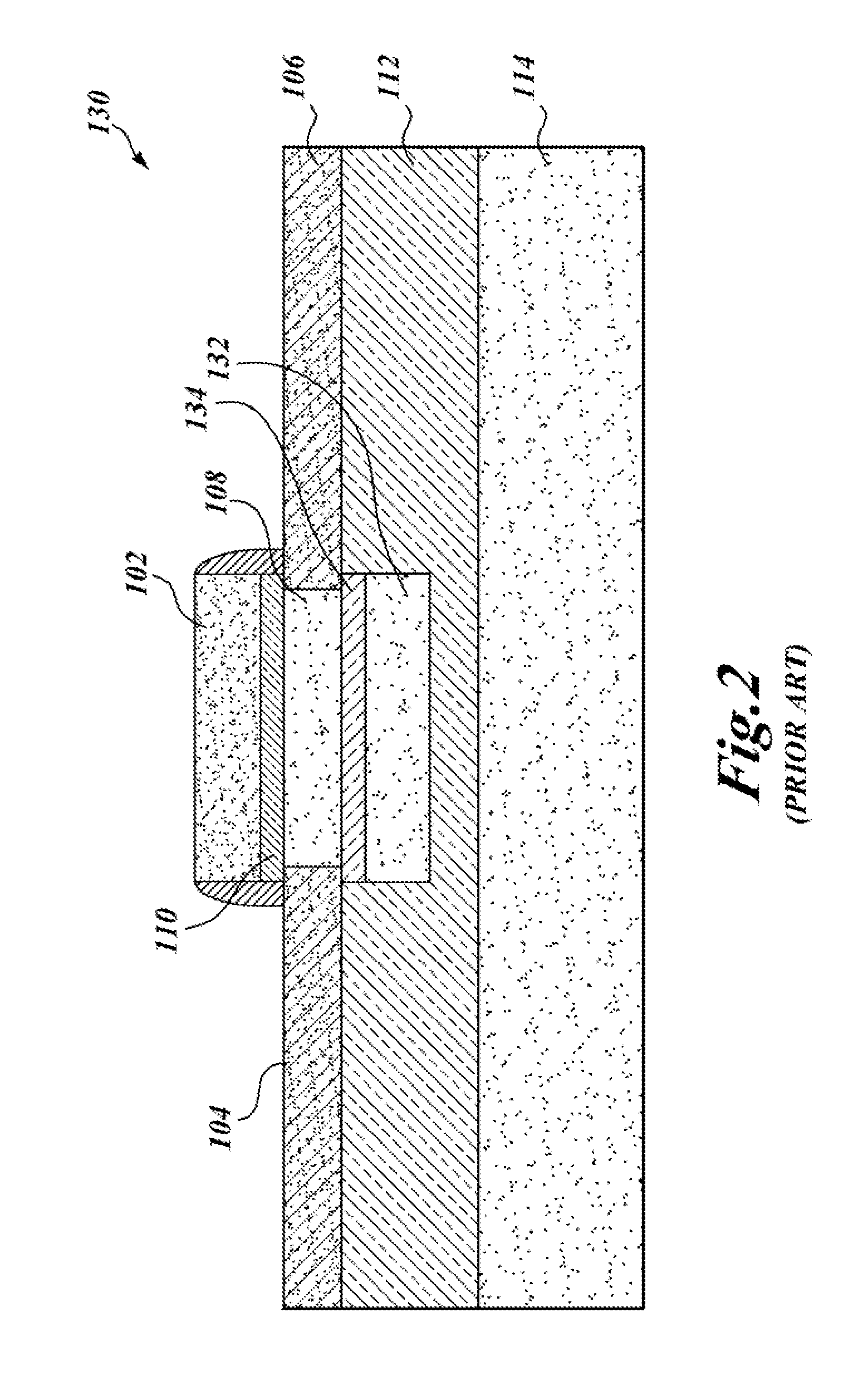
[0024]In the following description, certain specific details are set forth in order to provide a thorough understanding of various disclosed embodiments. However, one skilled in the relevant art will recognize that embodiments may be practiced without one or more of these specific details, or with other methods, components, materials, etc. In other instances, well-known structures associated with NMOS and PMOS transistors and associated circuits have not been shown or described in detail to avoid unnecessarily obscuring descriptions of the embodiments.

[0025]Unless the context requires otherwise, throughout the specification and claims which follow, the word “comprise” and variations thereof, such as, “comprises” and “comprising” are to be construed in an open, inclusive sense, that is as “including, but not limited to.”

[0026]Reference throughout the specification to “one embodiment” or “an embodiment” means that a particular feature, structure, or characteristic described in connect...


PUM


Abstract

Circuit module designs that incorporate dual gate field effect transistors are implemented with fully depleted silicon-on-insulator (FD-SOI) technology. Lowering the threshold voltages of the transistors can be accomplished through dynamic secondary gate control in which a back-biasing technique is used to operate the dual gate FD-SOI transistors with enhanced switching performance. Consequently, such transistors can operate at very low core voltage supply levels, down to as low as about 0.4 V, which allows the transistors to respond quickly and to switch at higher speeds. Performance improvements are shown in circuit simulations of an inverter, an amplifier, a level shifter, and a voltage detection circuit module.

Description

CROSS-REFERENCE TO RELATED APPLICATION[0001]The present patent application is a continuation-in-part of U.S. patent application Ser. No. 14 / 078,236, filed on Nov. 12, 2013, which is hereby incorporated by reference in its entirety.BACKGROUND[0002]1. Technical Field[0003]The present disclosure relates to dual gate transistors built on substrates having a buried oxide layer and, in particular, to the use of such dual gate transistors in integrated circuits to improve circuit performance.[0004]2. Description of the Related Art[0005]Integrated circuits typically incorporate N-doped and P-doped metal oxide semiconductor field effect transistor (MOSFET) devices in which current flows through a semiconducting channel between a source and a drain, in response to a bias voltage applied to a gate. When the applied voltage exceeds a characteristic threshold voltage Vt, the device switches on. Ideally, such a switch: a) passes zero current when it is off; b) supplies large current flow when it ...

Claims


Application Information

Patent Timeline
IPC IPC(8): H01L27/12H01L29/78H01L21/265H01L21/8238H01L21/762H01L21/266H01L27/092H01L21/84
CPCH01L27/1203H01L27/092H01L29/7831H01L21/265H01L21/823871H01L21/7624H01L21/266H01L21/84H01L29/78648H01L21/26513H01L21/31111H01L29/0649H01L29/51H01L29/517H01L29/66484
Inventor KUMAR, ANANDAGRAWAL, ANKIT
Owner STMICROELECTRONICS INT NV
Why Eureka
Try Eureka