Vertical resistive random access memory device, and method for manufacturing same

a random access memory and vertical resistive technology, applied in the direction of bulk negative resistance effect devices, semiconductor devices, electrical appliances, etc., can solve the problems of reram having a considerable drawback in reproduction, small deviation in operating voltage, current, durability, etc., to achieve stably operating resistance change memory, reduce manufacturing costs, and increase integration

Inactive Publication Date: 2015-06-11
INTELLECTUAL DISCOVERY CO LTD
View PDF1 Cites 17 Cited by
  • Summary
  • Abstract
  • Description
  • Claims
  • Application Information

AI Technical Summary

Benefits of technology

[0039]According to the exemplary embodiments of the present invention, it is possible to implement the resistance change memory (ReRAM) without the separate selection device merely by forming the metal oxide layers having the threshold switching characteristics and the memory switching characteristics at the cross points at which the plurality of horizontal electrodes extending in the horizontal direction and stacked having the insulating layer therebetween and the vertical electrodes extending in the vertical direction meet each other, thereby minimizing the manufacturing costs.
[0040]Further, according to the exemplary embodiments of the present invention, it is possible to further increase the integration by disposing the metal oxide layers having both of the threshold switching characteristics and the memory switching characteristics between the vertical electrodes having the plurality of horizontal electrodes stacked therebetween and penetrating between the horizontal electrodes in the vertical direction.
[0041]Further, according to the exemplary embodiments of the present invention, it is possible to provide the cell structure capable of being commonly used by memory cells by extending the selection device function layer along the vertical electrode, in the vertically stacked resistance change memory in which the resistance change material layers are formed at the cross points at which the plurality of horizontal electrodes extending in the horizontal direction and stacked having the insulating layer therebetween and the vertical electrodes extending in a vertical direction meet each other.
[0042]According to the exemplary embodiments of the present invention, it is possible to stably operate the resistance change memory by providing the sufficient current density for the resistance state change of the resistance change material layer by making the area of the selection device be sufficiently wider than that of the resistance change material layer. Further, according to the exemplary embodiments of the present invention, it is possible to minimize the contact area between the resistance change material layer and the electrode by providing the contact between the resistance change material layer and the horizontal electrode through the fine gap of the thin film layer formed between the resistance change material layer and the horizontal electrode, in the vertical resistance change memory in which the resistance change material layers are formed at the cross points at which the plurality of horizontal electrodes extending in the horizontal direction and stacked having the insulating layer therebetween and the vertical electrodes extending in a vertical direction meet each other, thereby stably operating the resistance change memory.
[0043]Further, according to the exemplary embodiments of the present invention, it is possible to improve the switching uniformity of the resistance change material layer by configuring the horizontal electrode in the multi-layer using the conductive materials having the different etch selectivities to have the lightening rod structure, in the vertical resistance change memory in which the resistance change material layers are formed at the cross points at which the plurality of horizontal electrodes extending in the horizontal direction and stacked having the insulating layer therebetween and the vertical electrodes extending in a vertical direction meet each other, thereby stably operating the resistance change memory.
[0044]Further, according to the exemplary embodiments of the present invention, it is possible to drive the ReRAM device without the selection device by configuring the resistance change material layers, which are formed at the cross points at which the plurality of horizontal electrodes extending in the horizontal direction and stacked having the insulating layer therebetween and the vertical electrodes extending in the vertical direction meet each other, as the first resistance change material layer and the second resistance change material layer which are made of different materials and forming the conducting filament by the metal material different from the first resistance change material layer, within the first resistance change material layer, thereby minimizing the manufacturing costs and improving the integration.

Problems solved by technology

Particularly, since a flash memory device which is a nonvolatile memory which has recently come into the limelight has a difficulty in scaling, to develop a next-generation terabit nonvolatile memory, the development of a memory device based on a new characteristic material for a semiconductor device is urgently required.
Second, the other of the two switching models is a switching model due to a lot of traps which are present inside the metal oxide.
Despite the merits, an accurate switching mechanism of the ReRAM is not yet known and therefore the ReRAM has a considerable drawback in reproduction, and further has a slight deviation in operating voltage, current, durability, and the like among devices.
The related art may improve integration by forming a ReRAM cell at the cross point between the vertical electrode and the horizontal electrode, but has a drawback in that a manufacturing process is still complicated.
However, the transistor has a limitation in a size reduction of the device due to a short channel effect like a punch through.
Further, the diode makes a current flow only in one direction and therefore may not be appropriate for a bipolar device exhibiting resistance change characteristics at both polarities like the ReRAM device.
However, the selection devices proposed until now may not provide a sufficient current to operate the resistance change material layer due to a small current density.
That is, the ReRAM clearly has two different resistance states, but has an excessively wide range of voltage in which the two resistance states start to change.
As such, when the distribution of voltage which causes the change in resistance is wide, it is difficult to reproduce the change in resistance of the resistance change material layer in a limited range of voltage.
This means that the resistance change material layer needs to have the same resistance state at the same applied voltage but may not actually have it.

Method used


Image

  • Vertical resistive random access memory device, and method for manufacturing same
  • Vertical resistive random access memory device, and method for manufacturing same
  • Vertical resistive random access memory device, and method for manufacturing same

Examples


Embodiment Construction

[0060]The foregoing objects, features, and advantages will become more apparent from the following detailed description of preferred embodiments of the present invention with reference to accompanying drawings, which are set forth in detail hereinafter, and therefore those skilled in the art may easily practice the technical ideas of the present invention. Further, in describing the present invention, when a detailed description of a well-known technology relating to the present invention may unnecessarily make the spirit of the present invention unclear, the detailed description thereof will be omitted. Hereinafter, exemplary embodiments of the present invention will be described in detail with reference to the accompanying drawings.

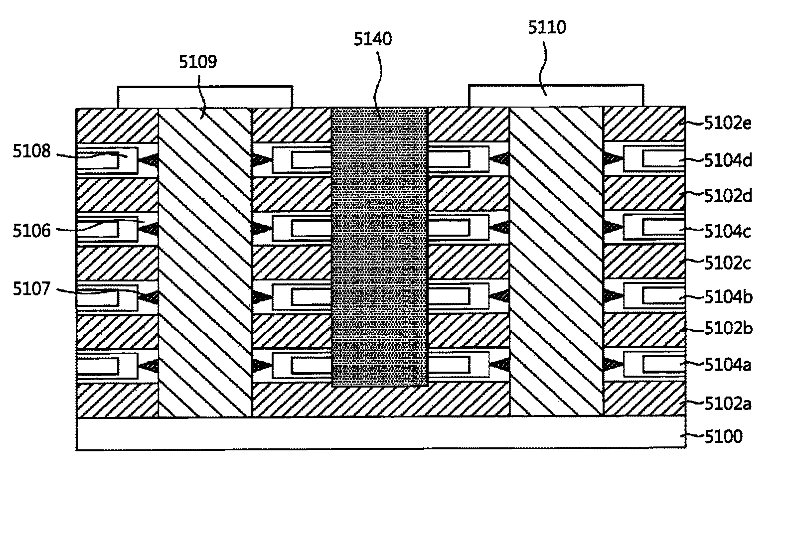
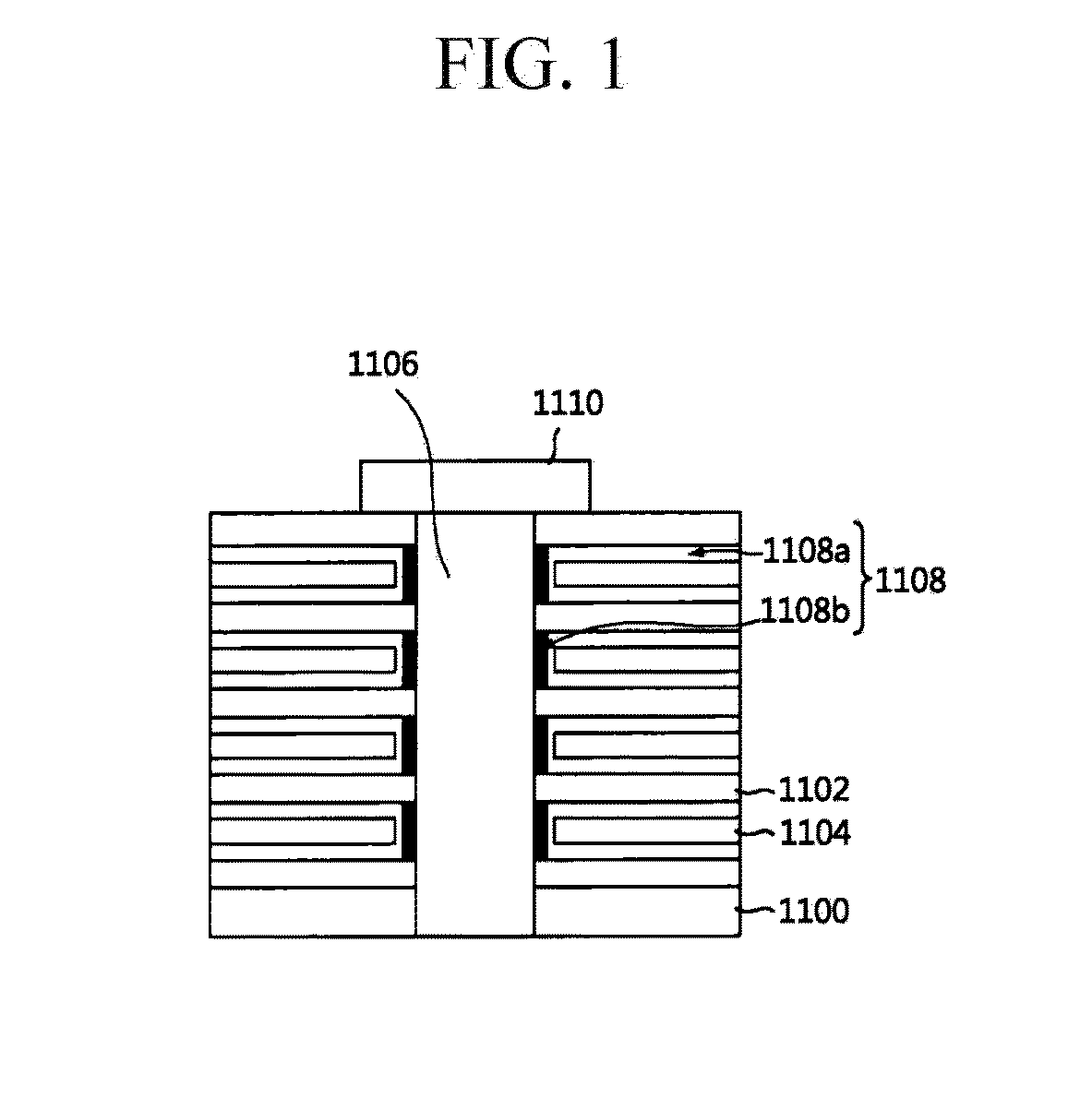
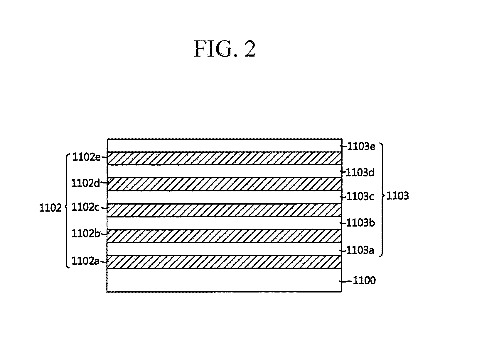
[0061]FIG. 1 is a cross-sectional view of a vertically stacked resistance change memory device according to an exemplary embodiment of the present invention. Referring to FIG. 1, insulating layers 1102 and horizontal electrodes 1104 are alternately stac...


PUM


Abstract

The present invention relates to a resistance change memory device and a method for manufacturing the same. According to an exemplary embodiment of the present invention, the resistance change memory device includes: a plurality of horizontal electrodes configured to be stacked at a predetermined interval from each other and extended in a horizontal direction; inter-layer insulating layers configured to each be formed between the plurality of horizontal electrodes; a plurality of vertical electrodes configured to have cross points with the horizontal electrodes by penetrating through the plurality of stacked horizontal electrodes and the inter-layer insulating layers in a vertical direction; and a metal oxide layer configured to have a U-shaped section in a form enclosing the horizontal electrode between the inter-layer insulating layer and the horizontal electrode and to make an oxygen composition ratio of a surface contacting the vertical electrode be higher than that of a surface contacting the horizontal electrode by performing oxygen treatment on the vertical electrode to have threshold switching characteristics and memory switching characteristics.

Description

TECHNICAL FIELD[0001]The present invention relates to a vertically stacked resistance change RAM (ReRAM), and more particularly, to a ReRAM device and a method for manufacturing the same capable of improving integration by forming a metal oxide layer having threshold switching characteristics and memory switching characteristics at cross points at which a plurality of horizontal electrodes extending in a horizontal direction and stacked having an insulating layer therebetween and vertical electrodes extending in a vertical direction meet each other.BACKGROUND ART[0002]With the development of the electronics industry, particularly the PC industry and the communications industry due to the development of an information industry, mobile devices have been developed. That is, as the PC industry and the communications industry have expanded, rapid high performance and multi-functionality surpassing existing speed of technical development have been required.[0003]In the traditional viewpoi...

Claims


Application Information

Patent Timeline
Patent Type & Authority Applications(United States)
IPC IPC(8): H01L27/24H01L45/00
CPCH01L27/2481H01L45/1233H01L45/1608H01L45/146H01L45/08H01L45/1253H10B63/22H10B63/845H10N70/24H10N70/245H10N70/823H10N70/8833H10N70/041H10B63/84H10N70/021H10N70/826H10N70/841
Inventor HWANG, HYUN-SANG
Owner INTELLECTUAL DISCOVERY CO LTD
Why Eureka
Try Eureka