Non-Volatile Memory and Methods for Producing Same

a non-volatile memory and non-volatile technology, applied in the direction of semiconductor devices, electrical apparatus, transistors, etc., can solve the problems of large operating current required during the erasing operation, leakage current from the source to the substrate, and difficulty in integration of the whole circuit, so as to reduce the per unit area of the memory unit, reduce the leakage current, and reduce the effect of per unit area

Inactive Publication Date: 2015-07-30
XINNOVA TECH
View PDF3 Cites 8 Cited by
  • Summary
  • Abstract
  • Description
  • Claims
  • Application Information

AI Technical Summary

Benefits of technology

[0008]An objective of the present invention is to overcome the drawbacks of the conventional techniques by providing a non-volatile memory which can reduce the leakage current resulting from the gate-induced drain leakage effect, ...

Problems solved by technology

Firstly, an over erasure effect exists.
When the memory unit undergoes the erasing operation, excessive electrons could be removed from the floating gate, resulting in a negative threshold voltage of an equivalent transistor component in the memory unit; namely, the memory unit is normally in a conductive state that leads to unnecessary leakage current.
Secondly, a larger operating current is required during the erasing operation.
When the memory undergoes the erasing operation, the source voltage is much larger than the voltage of the floating gate and, thus, results in a gate-induced drain leakage (GIDL) effect, leading to leakage current from the source to the substrate.
As a result, an external power source more powerful in providing current is required in the operation, leading to difficulties in integration of the whole circuit.
However, as the processes are more and more advanced and the size becomes smaller and smaller, the li...

Method used


Image

  • Non-Volatile Memory and Methods for Producing Same
  • Non-Volatile Memory and Methods for Producing Same
  • Non-Volatile Memory and Methods for Producing Same

Examples


Embodiment Construction

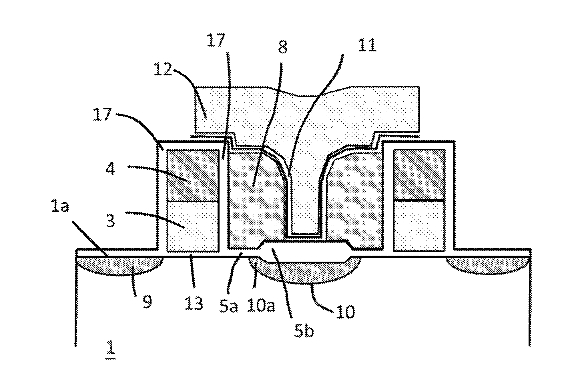
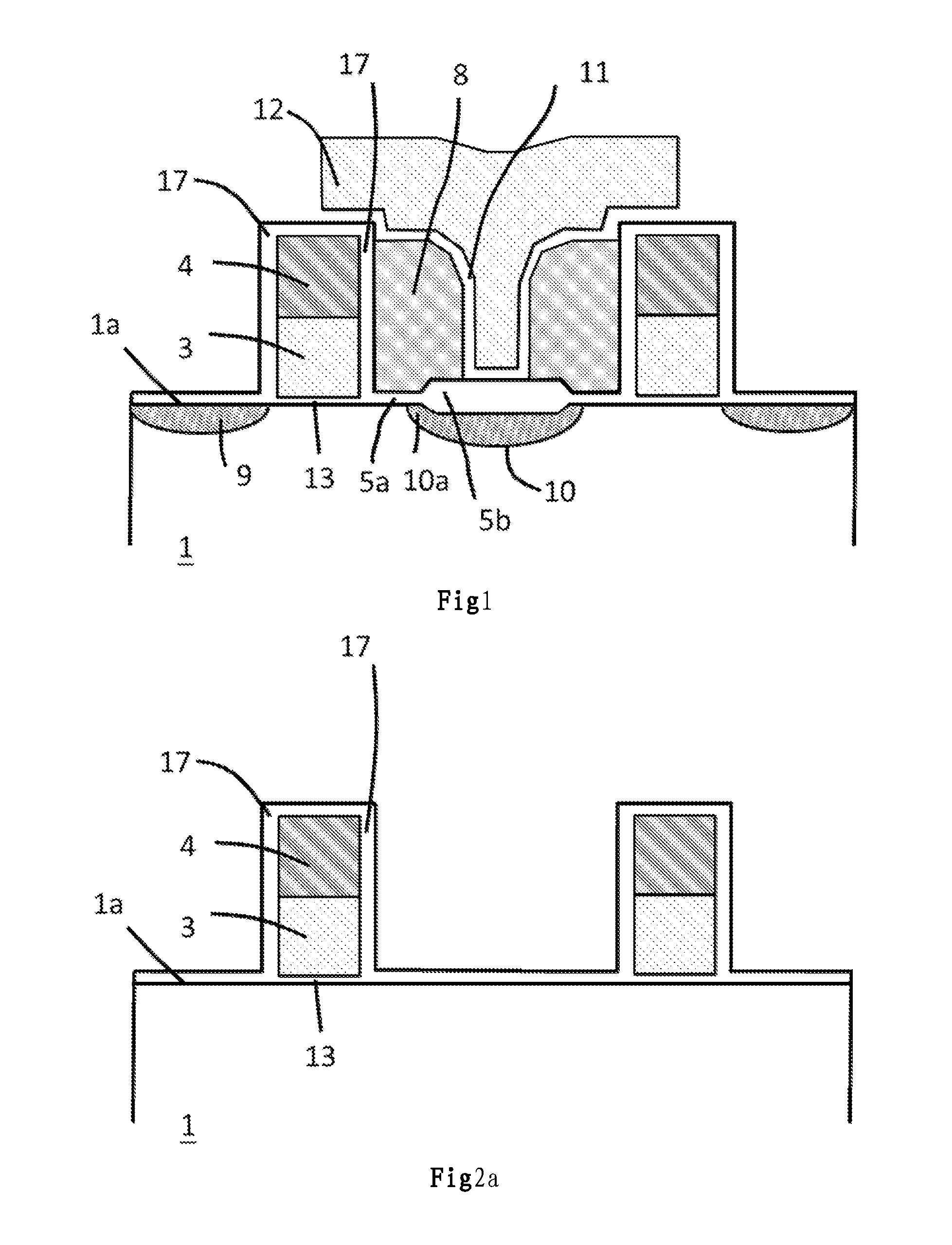
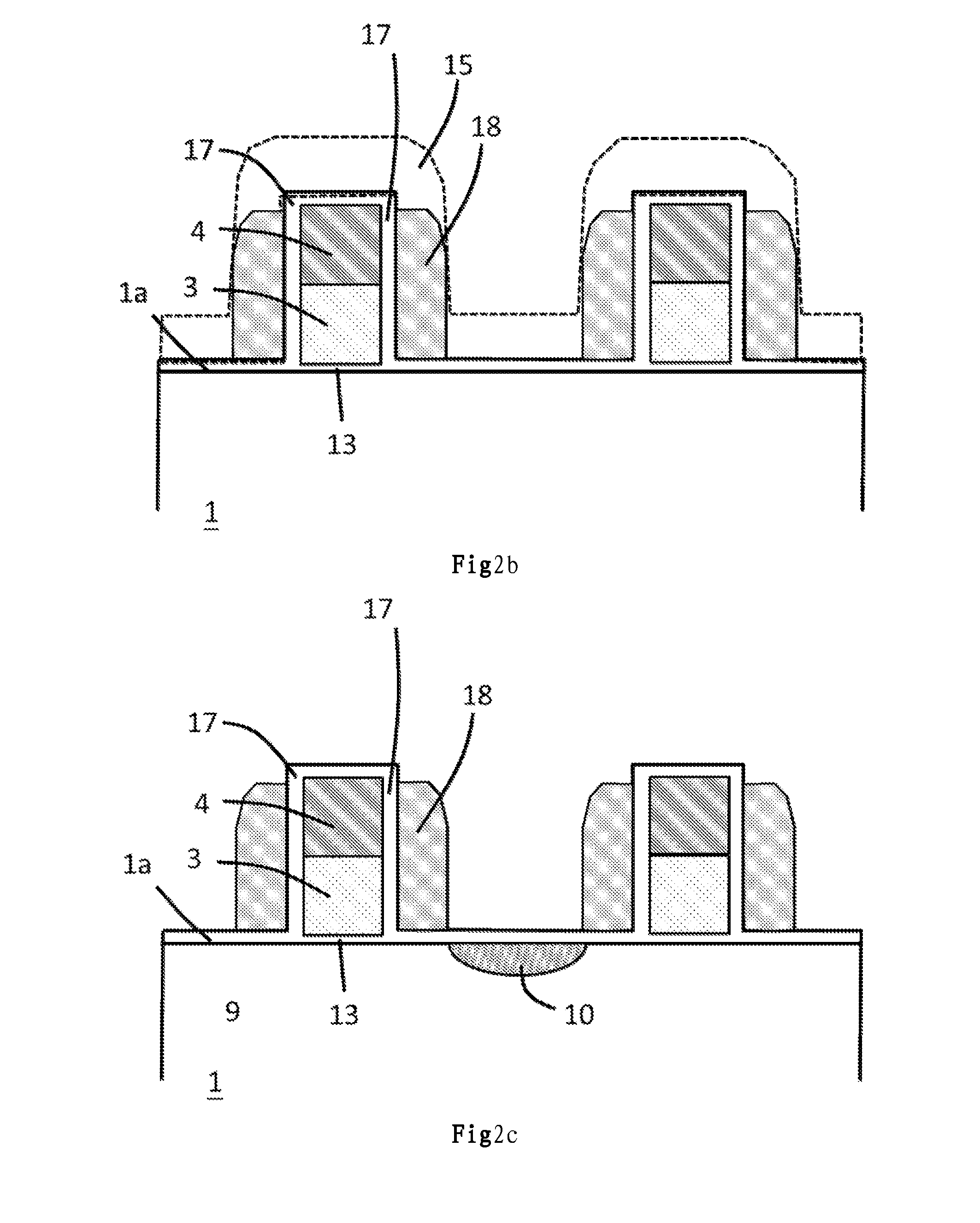
[0087]The present invention will be further described by way of examples in connection with the accompanying drawings.

[0088]The technical terms in the following description are used in reference to the idioms in the art. Some of the terms are explained or defined in the specification, and such explanation or definition in the specification should be based to interpret these terms. Furthermore, on the premise of practicability, the terms “on”, “under”, “at”, etc. used in the specification refers to directly or indirectly “on” or “under” an object or a reference object and directly or indirectly “at” an object or a reference object. The term “indirect” used herein refers to the existence of an intermediate object or a physical space. On the premise of practicability, the terms “contiguous” and “between” used herein refers to two objects or two reference objects between which an intermediate object or a space exists or does not exist. Furthermore, in the following description related t...


PUM


Abstract

A non-volatile memory unit includes a substrate on which a source diffusion region and a drain diffusion region are formed. A first dielectric layer and a tunnel dielectric layer are formed between the source diffusion region and the drain diffusion region, are respectively on the drain diffusion region side and the source diffusion region side, and are connected to each other. A select gate is formed on the first dielectric layer. A source insulating layer is formed on the source diffusion region. The tunnel dielectric layer extends to the source diffusion region and is connected to the source insulating layer. A floating gate is formed on a face of the tunnel dielectric layer and a face of the thicker source insulating layer. A control gate is formed on the floating gate. The control gate and the floating gate are insulating to each other by the second dielectric layer.

Description

BACKGROUND OF THE INVENTION[0001]The present invention relates to a structure of an integrated circuit component and its producing methods and, more particularly, to a non-volatile memory and methods for producing the non-volatile memory.[0002]Non-volatile memories have advantages of small volumes, light weights, low power consumption, and prevention of loss of data resulting from power interruption and are, thus, suitable for applications in hand-held electronic devices. Following the popularization of hand-held electronic devices, non-volatile memories have widely been used as multimedia storage devices or used for maintaining normal operation of electronic systems. The need of non-volatile memories increases every year, and the costs and prices decrease, which is a positive cycle for non-volatile memories. Thus, non-volatile memories have become one of the most important products in the semiconductor industry.[0003]U.S. Pat. No. 4,698,787 discloses a non-volatile memory unit of a...

Claims


Application Information

Patent Timeline
IPC IPC(8): H01L29/423H01L27/115H01L29/66H01L29/788
CPCH01L29/42324H01L29/66825H01L27/11521H01L29/788H01L29/42328H01L29/7884H01L29/40114H10B41/30
Inventor FAN, DER-TSYRCHEN, CHIH-MINGLU, JUNG-CHANG
Owner XINNOVA TECH
Why Eureka
Try Eureka