Process and method for in-situ dry cleaning of thin film deposition reactors and thin film layers

a technology of thin film deposition reactor and in-situ dry cleaning, which is applied in the direction of electrostatic cleaning, chemical vapor deposition coating, ion implantation coating, etc., can solve the problems of contaminated reactant gases flowing through the reactor chamber, low yield or complete loss of wafers, and time-consuming, etc., to achieve efficient dry etching

Active Publication Date: 2015-08-06
SEASTAR CHEM
View PDF6 Cites 334 Cited by
  • Summary
  • Abstract
  • Description
  • Claims
  • Application Information

AI Technical Summary

Benefits of technology

[0025]An advantage of the invention is the simple use of pure compounds or gas mixtures to generate the cleaning compounds in-situ. The new process relies on thermal or light activation to achieve efficient dry etching.
[0026]In one aspect, the invention comprises a method for cleaning reaction product deposits from interior surfaces of a chemical reactor chamber or from a substrate within the chemical reactor chamber, comprising the steps of heating the reactor chamber to an elevated temperature; introducing an etchant gas into the reactor chamber, activating the etchant gas; allowing an etching reaction to proceed between the etchant gas and the reaction product deposits; and evacuating the etchant gas together with gaseous products of the etching reaction.
[0027]The etchant gas may be of the general formula AOmXn, wherein A is selected from the group consisting of C, N, and S; O is oxygen; X is a halogen; and the subscripts m and n are greater than zero. Alternatively, the etchant gas may be of the general formula AOmXnYp, wherein A is selected from the group consisting of C, N, and S; O is oxygen; X and Y are different halogens; and the subscripts m, n and p are greater than zero. As another alternative, the etchant gas may be of the general formula AmXn, wherein A is selected from the group consisting of C, N, and S; X is a halogen; and the subscripts m and n are greater than zero.
[0028]In another aspect, the invention comprises the further step of generating the etchant gas prior to the introduction into the chamber. This generation may take the form of bubbling a carrier gas through a plurality of liquid chemical constituents and then combining the resulting gases, and / or mixing two or more chemical constituent gases. Alternatively or in addition, the carrier gas may be bubbled through a liquid chemical constituent to volatilize the liquid chemical constituent into the etchant, prior to the introduction of the etchant gas into the chamber.
[0029]In yet a further aspect, the invention may comprise activating the etchant gas by exposing it to an activation mechanism in a gas activation chamber prior to introduction into the reactor chamber. The gas activation mechanism may be any one or more of heat, ultraviolet light and plasma discharge. Alternatively, the etchant gas may be activated by exposing it to a thermal activation mechanism after introduction into the reactor chamber; the thermal activation mechanism being selected from the group consisting of the overall temperature within the reactor chamber and a local heat source within the reactor chamber.
[0030]In yet a further aspect, the etchant gas may also contain an additive. The additive may be a halogen gas, or it may be of the general formula RX, wherein R is selected from the group consisting of H and Me; and X is a halogen, selected from the group consisting of F, Cl, Br and I.

Problems solved by technology

The deposits will eventually start to delaminate, generating particles that can fall onto the substrate wafers, contaminating them and resulting in either low yield or complete loss of the wafers.
The reactant gases flowing through the reactor chamber may also be contaminated by the deposits.
Depending on the configurations and materials used in the reactor, effective cleaning may require complete reactor strip down and wet clean, which is time consuming and reduces reactor efficiency.
It can be difficult to clean deposits off all of these types of surfaces, without using different types of etchants or other cleaners.
Use of these highly reactive etchants is difficult as they are corrosive to components within the reactor vessel and require high temperatures.
Wet etching is disadvantageous in that it is time and labour consuming in comparison with dry reactive gas etching.

Method used


Image

  • Process and method for in-situ dry cleaning of thin film deposition  reactors and thin film layers
  • Process and method for in-situ dry cleaning of thin film deposition  reactors and thin film layers
  • Process and method for in-situ dry cleaning of thin film deposition  reactors and thin film layers

Examples


example 1

SOCl2 200° C.

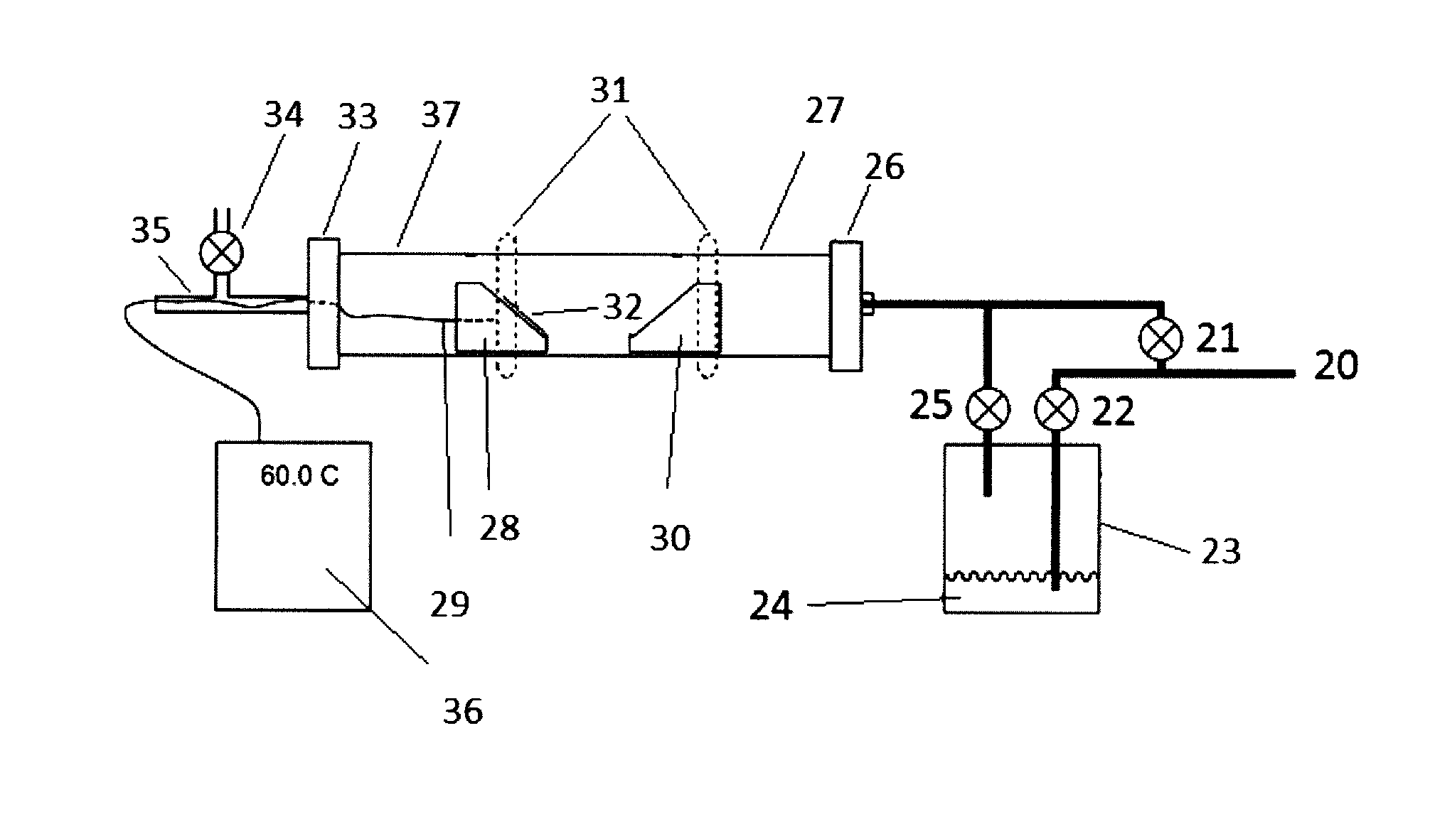
[0049]A coated substrate 32 was placed on the first substrate holder 28. The substrate 32 was heated with IR heater 31 to 200° C. under a continuous carrier gas (Ar) flow through the reactor chamber 27 from the gas inlet 20 and direct input valve 21. Once the substrate reached a temperature of 200° C., the flow of the carrier gas was diverted through bubbler valve 22 into bubbler 23 containing reagent 24 (SOCl2), such that SOCl2 was picked up in the carrier gas, forming an etchant gas. The etchant gas entered the reactor chamber 27 through valve 25, passed over the substrate 32 and etched away the deposit on the stainless steel substrate 32. The reaction was very rapid over the first five minutes, and then proceeded more slowly, such that the etching process took 10-13 minutes to clean the substrate to a shiny stainless condition. The by-products, which were mainly GaCl3 and SO2, were collected in the cooled area 37 of chamber 27.

example 2

SOBr2 200° C.

[0050]A coated substrate 32 was placed on the first substrate holder 28. The substrate 32 was heated with IR heater 31 to 200° C. under a continuous carrier gas (Ar) flow through the reactor chamber 27 from the gas inlet 20 and direct input valve 21. Once the substrate reached 200° C., the flow of the carrier gas was diverted through bubbler valve 22 into bubbler 23 containing reagent 24 (SOBr2), such that SOBr2 was picked up in the carrier gas, producing an etchant gas. The etchant gas entered the reactor chamber 27 through valve 25, passed over the substrate 32 and etched away the deposit on the stainless steel substrate 32. The reaction was very quick and efficient, cleaning the substrate completely within 7-9 minutes. The by-products, which were mainly GaBr3 and SO2, were collected in the cooled area 37 of chamber 27.

example 3

SOBr2 200° Preheat 300° C.

[0051]A coated substrate 32 was placed on the first substrate holder 28. The substrate 32 was heated with IR heater 31 to 200° C. under a continuous carrier gas (Ar) flow through the reactor chamber 27 from the gas inlet 20 and direct input valve 21. The second substrate holder 30 was heated to 300° C. with the IR heater 31. Once the appropriate temperatures were reached, the flow of the carrier gas was diverted through bubbler valve 22 into bubbler 23 containing reagent 24 (SOBr2), such that SOBr2 was picked up in the carrier gas, and an etchant gas was produced. The etchant gas entered the reactor chamber 27 through valve 25, was thermally activated as it passed over the substrate holder 30, passed over substrate 32 and etched away the deposit on the stainless steel substrate 32. The reaction was very quick and efficient, cleaning the substrate completely within 3-5 minutes. The by-products, which were mainly GaBr3 and SO2, were collected in the cooled ar...


PUM

PropertyMeasurementUnit
temperatureaaaaaaaaaa

Abstract

The invention relates to the use of thionyl chloride and related materials for dry etching of internal surfaces of metalorganic vapour phase epitaxy (MOVPE) reactors to remove deposits. The method is also useful for the dry etching of process substrates within such reactors for cleaning and processing of those substrates. The invention may be particularly adaptable to chemical vapor deposition reactors used in the manufacture of high brightness LED's based on III-V semiconductors such as GaN and related materials. Features of the process include thermal, UV, and plasma activated dry cleaning, and the use of etchant gases such as COCl2, COBr2, COl2, SOl2, SOCl2, SOBr2, SO2Cl2, SO2Br2, NOCI, NOBr, NOl, S2Cl2, S2Br2, SCI2, SBr2, SOClBr, SOClF and SOFBr, either formed from neat materials or combinations of constituent gases such as CO, SO, SO2 or NO with halogens, to achieve the desired effect.

Description

FIELD OF THE INVENTION[0001]The invention relates to a method, composition and apparatus for dry etching or cleaning of interior surfaces of thin film deposition reactors.BACKGROUND OF THE INVENTION[0002]Metalorganic vapour phase epitaxy (MOVPE), also known as organometallic vapour phase epitaxy (OMVPE) or metalorganic chemical vapour deposition (MOCVD), is an arranged chemical vapour deposition method. In MOVPE ultra-pure gases are injected into a reactor and finely dosed to deposit a very thin layer of atoms onto a semiconductor wafer. Surface reaction of organic compounds or metalorganics and hydrides containing the required chemical elements creates conditions for crystalline growth—epitaxy of materials and compound semiconductors. Unlike traditional silicon semiconductors, these semiconductors may contain combinations of Group III and Group V, Group II and Group VI, Group IV, or Group IV, V and VI elements.[0003]In the vapor phase epitaxy (VPE) technique, reactant gases are com...

Claims


Application Information

Patent Timeline
Patent Type & Authority Applications(United States)
IPC IPC(8): C23C16/44
CPCC23G5/00C23C16/4405H01L21/02046C23C14/564
Inventor ODEDRA, RAJESH
Owner SEASTAR CHEM
Why Eureka
Try Eureka