Low Electric Field Source Erasable Non-Volatile Memory and Methods for Producing Same
a non-volatile memory, low electric field technology, applied in the direction of semiconductor devices, electrical apparatus, transistors, etc., can solve the problems of large operating current required during the erasing operation, leakage current from the source to the substrate, and difficulties in the integration of the whole circuit, so as to avoid a high electric field
- Summary
- Abstract
- Description
- Claims
- Application Information
AI Technical Summary
Benefits of technology
Problems solved by technology
Method used
Image
Examples
first embodiment
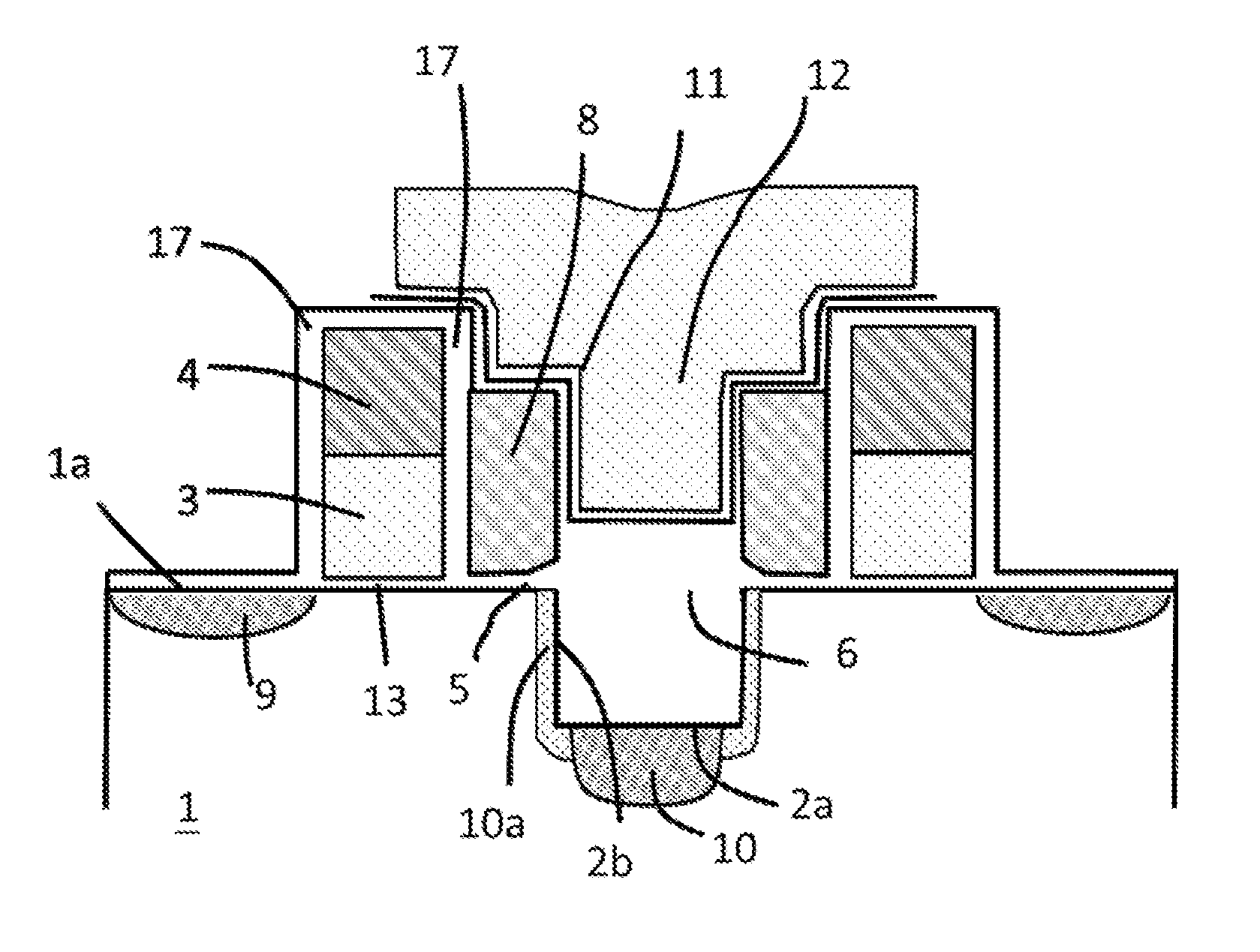
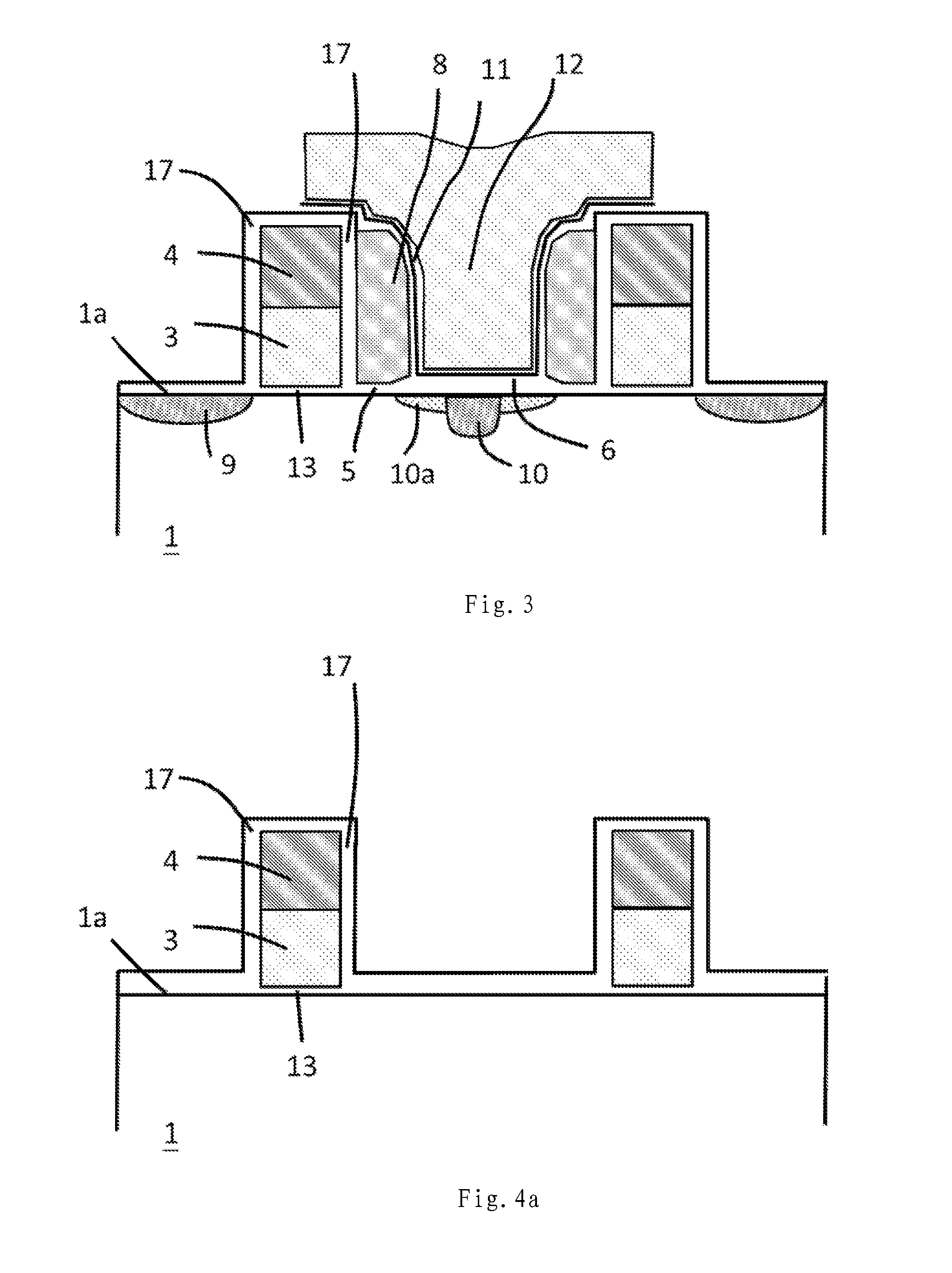
[0101]FIG. 3 is a diagrammatic cross sectional view of a low electric field source erasable non-volatile memory unit of a first embodiment according to the present invention.
[0102]Please refer to FIG. 3 showing two low electric field source erasable non-volatile memory units symmetric to each other. Description of the low electric field source erasable non-volatile memory unit at the left part of the figure will be set forth. The low electric field source erasable non-volatile memory unit includes a substrate that is generally a p-type silicon substrate 1. The p-type silicon substrate 1 includes an upper surface 1a. In the p-type silicon substrate 1, a drain diffusion region 9 is formed by an n-type doped layer, and a source diffusion region 10 is formed by another n-type doped layer. The source diffusion region 10 includes a lightly-doped region 10a that is a lightly-doped n-type region (source lightly n-doped diffusion). The drain diffusion region 9 is not contiguous to the source...
second embodiment
[0124]FIG. 5 is a diagrammatic cross sectional view of a low electric field source erasable non-volatile memory unit of a second embodiment according to the present invention.
[0125]An example of the method for producing the low electric field source erasable non-volatile memory unit of the second embodiment will now be set forth in connection with FIGS. 6a-6i.
[0126]The formation step shown in FIG. 6a is the same as that shown in FIG. 4a. Please refer to the corresponding description in connection with FIG. 4a.
[0127]The formation step shown in FIG. 6b is the same as that shown in FIG. 4b. Please refer to the corresponding description in connection with FIG. 4b.
[0128]As shown in FIG. 6c, a flat polycrystalline silicon layer 7 is formed on the face of the structure of FIG. 6b by chemical vapor deposition (CVD) and etch back or chemical-mechanical polishing (CMP). The upper face of the polycrystalline silicon layer 7 above the first insulating layer 4 and the floating gate 3 has an e...
PUM
 Abstract
Description
Claims
Application Information


