
Semiconductor device, and manufacturing method for same

a semiconductor device and manufacturing method technology, applied in semiconductor devices, semiconductor/solid-state device details, capacitors, etc., can solve the problems of increasing the contact resistance the surface area of contact between the capacitor contact plug and the capacitor contact pad, so as to reduce the contact resistance of the capacitor contact and increase the contact resistance

Inactive Publication Date: 2015-09-10
YOKOMICHI MASAHIRO
View PDF3 Cites 11 Cited by
  • Summary
  • Abstract
  • Description
  • Claims
  • Application Information

AI Technical Summary

Benefits of technology

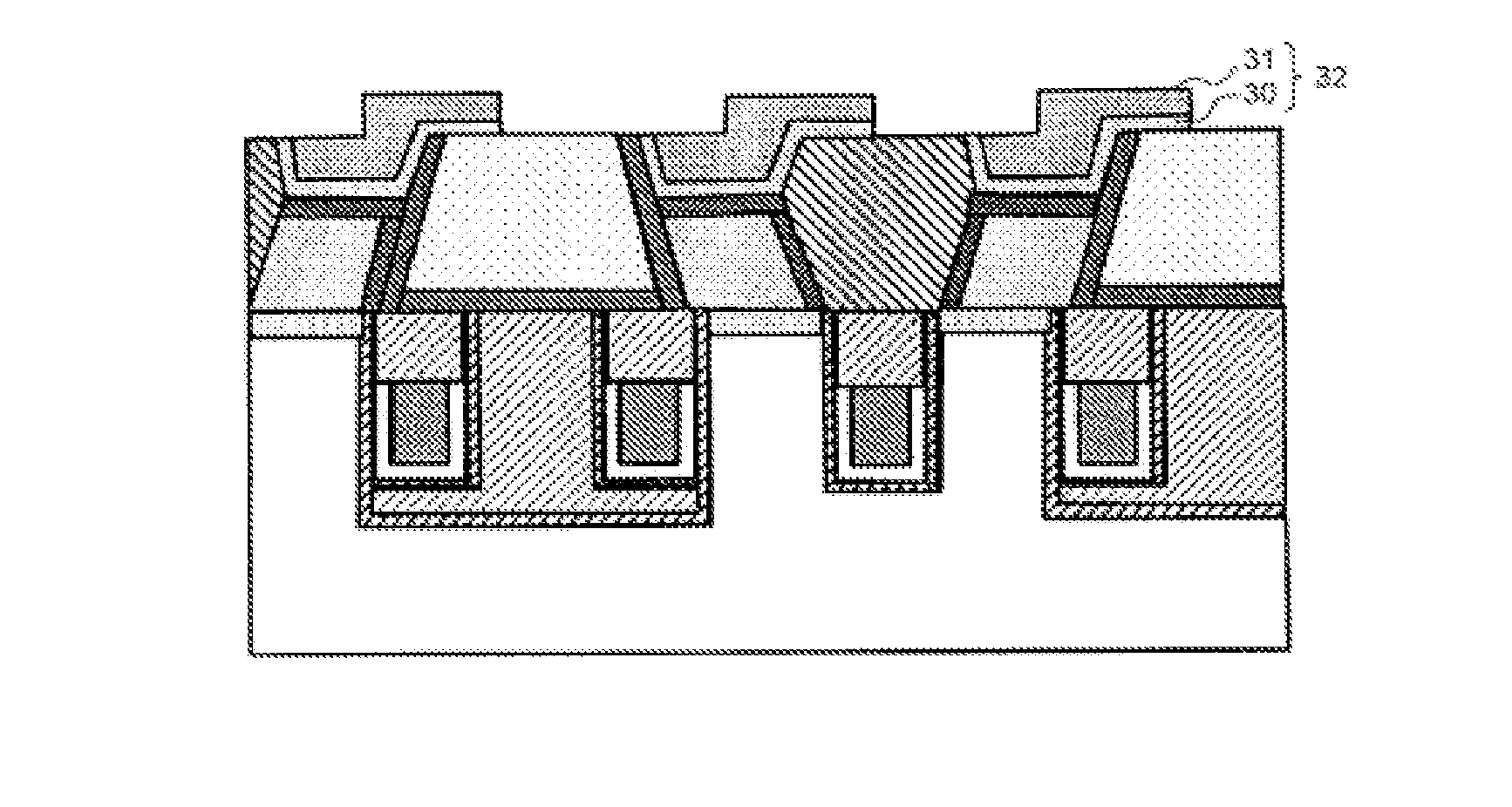
The present invention provides a low-resistance electrically-conductive film on the upper surfaces of plugs and on the side surfaces of plugs, reducing contact resistance with electrodes connected to the plugs and ensuring a constant level of contact even if the contact surface area between the plugs and pads connected to elements decreases. This invention helps to maintain a reliable electrical connection and minimize contact resistance.

Problems solved by technology

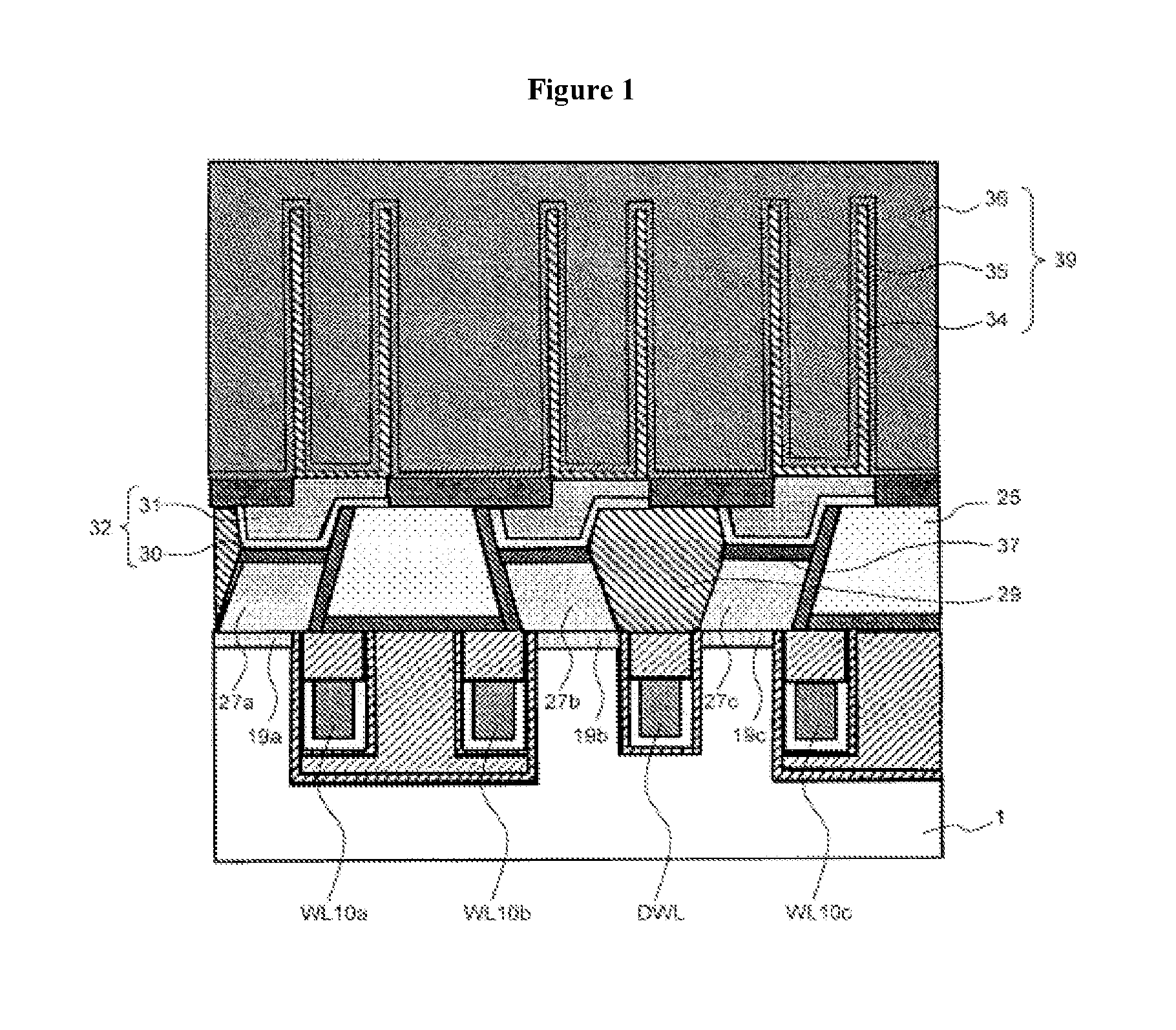
With this construction, however, if miniaturization progresses and the surface area of the upper surfaces of the capacitor contact plugs decreases, there is a problem in that the surface area of contact between the capacitor contact plugs and the capacitor contact pads, which are connected to the capacitor contact plugs by way of the cobalt silicide, also decreases, and the contact resistance thus increases.

Method used


Image

  • Semiconductor device, and manufacturing method for same
  • Semiconductor device, and manufacturing method for same
  • Semiconductor device, and manufacturing method for same

Examples


Embodiment Construction

[0048]The configuration of the semiconductor device in this mode of embodiment will now be described. This mode of embodiment assumes a case in which the semiconductor device is a DRAM.

[0049]FIG. 6 is a cross-sectional view illustrating a configuration example of a semiconductor device according to this mode embodiment. FIG. 6 illustrates part of a pattern of memory cell arrays. In the plan view illustrated in FIG. 6, the left-right direction is the X-axis direction, the up-down direction is the Y-axis direction, and the longitudinal direction of the pattern of active regions isolated by element isolation regions is the X′-axis direction.

[0050]As illustrated in FIG. 6, in a semiconductor substrate 1, element isolation regions 12 extending in the X′-axis direction, and active regions 13, also extending in the X′-axis direction, are disposed alternately at equal intervals and with an equal pitch in the Y-direction. The element isolation regions 12 are formed by an element isolation i...


PUM


Abstract

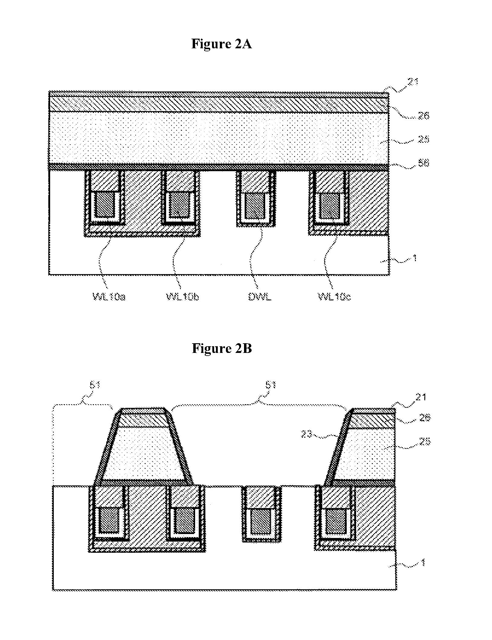
This method for manufacturing a semiconductor device comprises: a step for forming a first groove (51) that extends in a prescribed direction in a first insulating layer (25) on a semiconductor substrate (1); a step for forming an electrically conductive embedded layer (127) in the first groove; a step for forming a first and second plug (27b, 27c) by dividing the embedded layer in a prescribed direction; a step for forming a first conductive film (55), having lower resistance than the embedded layer, on the exposed side surfaces of the first and second plugs; a step for embedding a second insulating layer (29) in a second groove that is located between the first conductive films of the first and second plugs; and a step for forming a second conductive film (37), having lower resistance than the embedded layer, on the exposed top surfaces of the first and second plugs.

Description

TECHNICAL FIELD[0001]The present invention relates to a semiconductor device and a method for manufacturing the same.BACKGROUND ART[0002]Patent literature article 1 discloses one configuration example of a DRAM (Dynamic Random Access Memory), as a semiconductor device.[0003]The configuration of a memory cell in a DRAM will be described with reference to FIG. 1. FIG. 1 is a cross-sectional view illustrating one configuration example of a related semiconductor device.[0004]Word lines WL10a to WL10c connected to gate electrodes of MOS (Metal Oxide Semiconductor) transistors, and a dummy word line DWL which isolates active regions, are provided in a semiconductor substrate 1. Impurity-diffused layers 19a to 19c which form one electrode, from the source electrode and the drain electrode, of the MOS transistor are connected to capacitors 39 by way of capacitor contact plugs 27a to 27c and capacitor contact pads 32.[0005]Impurity-diffused layers (which are not shown in the drawing) which f...

Claims


Application Information

Patent Timeline
Patent Type & Authority Applications(United States)
IPC IPC(8): H01L27/108H01L23/532H01L21/3205H01L23/528H01L21/768H01L21/3213
CPCH01L27/10855H01L21/76802H01L21/76877H01L21/32139H01L21/76886H01L23/53209H01L27/10823H01L21/76897H01L21/32053H01L23/528H01L23/53271H01L21/76837H01L28/90H01L21/31144H01L2924/0002H10B12/315H10B12/34H10B12/488H10B12/0335H01L21/76883H01L2924/00H01L21/76895
Inventor YOKOMICHI, MASAHIRO
Owner YOKOMICHI MASAHIRO
Learn More