Point source light-emitting diode

Active Publication Date: 2015-09-10
DAIDO STEEL CO LTD
View PDF3 Cites 1 Cited by
  • Summary
  • Abstract
  • Description
  • Claims
  • Application Information

AI Technical Summary

Benefits of technology

The present invention provides a point source light-emitting diode that reduces side light from its ends. This is achieved by designing a topside electrode with a specific distance between its outer edges. The technical effect is an improved suppression of side light, resulting in more efficient and controlled light emission.

Problems solved by technology

There have been cases where the side light rays leaking out from the end faces of the chip had an intensity of, for example, about 20% of the maximum intensity, and besides, they caused a trouble of mixing with output light given off via the aperture formed in the topside electrode of the point source light-emitting diode as a noise component.
In some cases, this noise component is an impediment to performing measurements or communications utilizing the point source light-emitting diodes as light sources.
However, there have been cases where formation of side walls in uniform thickness was difficult to end in failure to suppress side light reliably.

Method used


Image

  • Point source light-emitting diode
  • Point source light-emitting diode
  • Point source light-emitting diode

Examples


embodiment 1

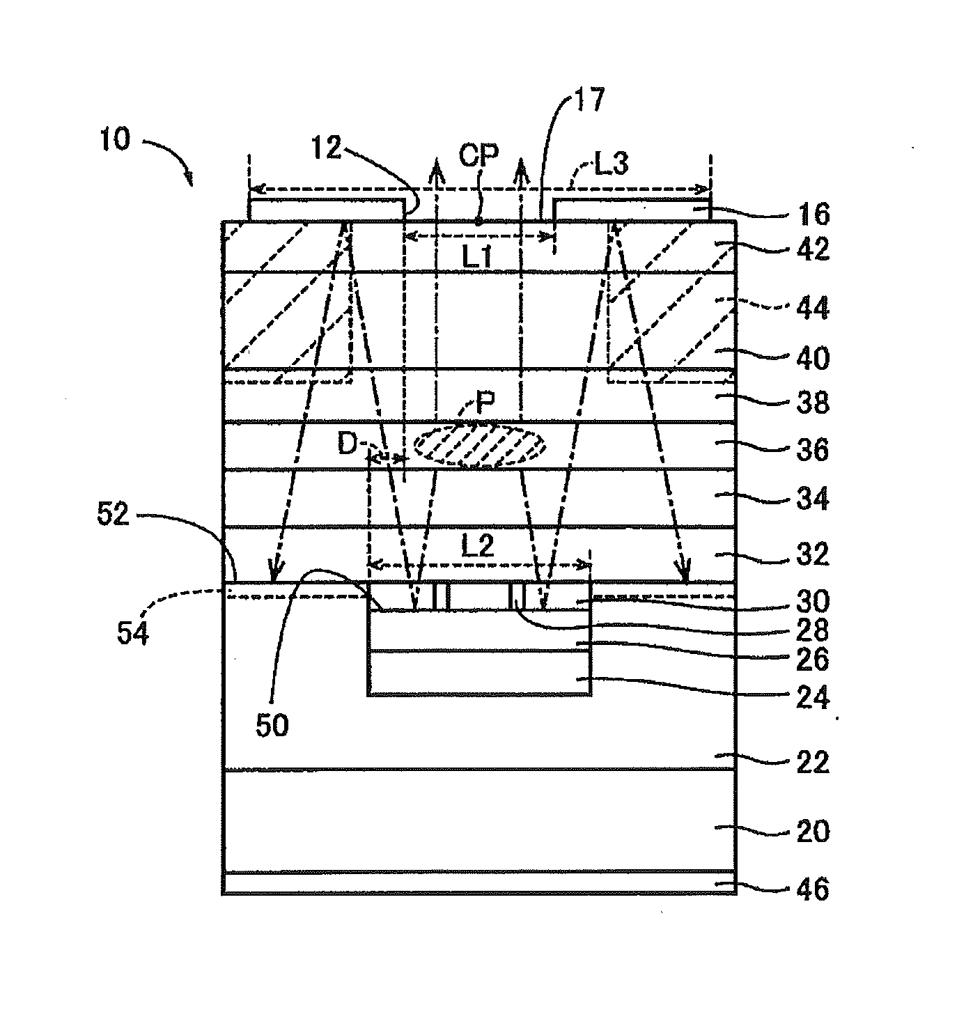
[0029]FIG. 1 is a plan view illustrating a surface emission-type semiconductor light-emitting element to which the present invention has been applied, that is, a point source light-emitting diode 10. And FIG. 2 is a diagram illustrating a vertical cross section passing through the central point CP of the aperture 12 formed in the topside electrode 16 of the point source light-emitting diode 10, and this diagram is a cross section viewed from the direction along the arrow of the II-II line in FIG. 1. The point source light-emitting diode 10 is a chip-shaped rectangular solid having on its top face not only a topside electrode 16 provided with a locally-formed nearly square aperture 12 and a locally-formed bonding pad 14 but also a light extraction face 17 embraced in the bosom of the aperture 12. The topside electrode 16 is stuck by means of, for example, vapor deposition or sputtering. The topside electrode 16 is formed from, for example, an AuGeNi eutectic alloy. In the interior of...

embodiment 2

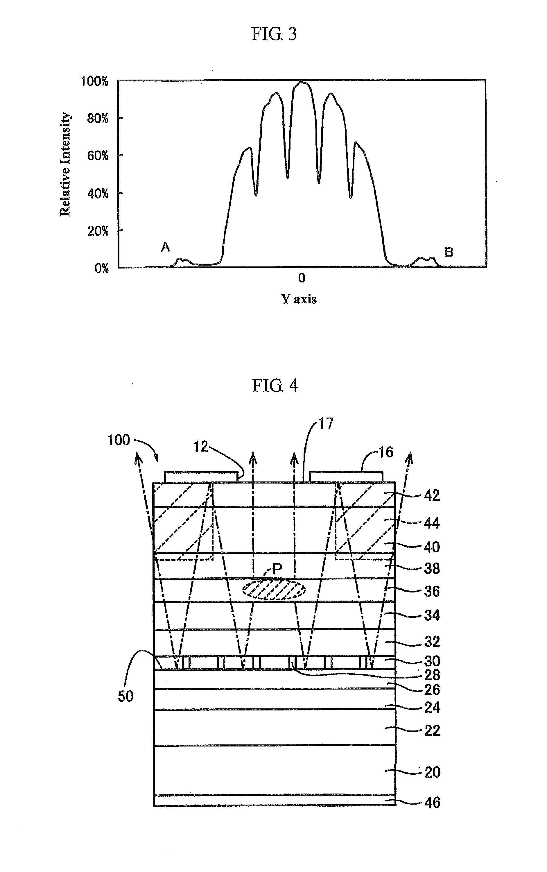
[0054]In FIG. 8 is illustrated a structural example of a point source light-emitting diode 70 of a form in which the dielectric layer 30 is provided locally at the place corresponding to the aperture 12 in the same manner as in the point source light-emitting diodes 10, but each of the metal layer 26 and the diffusion-control barrier layer 24 is provided all over a traverse plane of the diode chip, parallel to the topside electrode 16. In the point source light-emitting diode 70, the metal layer 26 and the first contact layer 32 immediately adjoin each other around the dielectric layer 30, and react with each other due to the heat at the time of thermocompression bonding of the support substrate 20, thereby forming a light reflection reduction face 52. Thus, the point source light-emitting diode 70 according to this embodiment can achieve the same operational advantages as the point source light-emitting diode 10.

[0055]In the foregoing, representative embodiments according to the pr...


PUM


Abstract

The present invention relates to a point source light-emitting diode containing a support substrate, a metal layer, a first conduction-type layer, an active layer, a second conduction-type layer containing a current-narrowing structure, and a topside electrode having an aperture, stacking in this order, in which the metal layer is provided locally in an area corresponding to the aperture and has a metal reflection face by which a light generated in the active layer is reflected towards the aperture side, and the point source light-emitting diode further contains a light-reflection reduction face having a lower reflectivity and / or a higher absorptivity than the metal reflection face, provided around the metal reflection face.

Description

FIELD OF THE INVENTION[0001]The present invention relates to a point source light-emitting diode having a chip structure that suppresses side light leakage from end faces of the chips.BACKGROUND ART OF THE INVENTION[0002]There have been known chip-shaped light-emitting diodes having an active layer between a topside electrode and a support substrate, a current-narrowing structure designed so as to centralize driving current in a certain region of the active layer and to induce local emission of light from the certain region of the active layer, and a metal reflection layer for making the light emitted from the active layer toward the substrate side be reflected toward the side of the topside electrode, in which output light is given off via an aperture locally formed in the topside electrode. An example of them is the light-emitting diode disclosed in Patent Document 1. In such a light-emitting diode, among the light rays produced in the active layer, light ray directed to the side ...

Claims


Application Information

Patent Timeline
IPC IPC(8): H01L33/10H01L33/38H01L33/58
CPCH01L33/10H01L33/38H01L33/58H01L33/145H01L33/387H01L33/405
Inventor HIROTANI, MASUMIIIO, SHINJISONE, HIDETOSHIKAWAGUCHI, KEIZOYANG, CHENG CHUNG
Owner DAIDO STEEL CO LTD
Why Eureka
Try Eureka