Grating coupler for inter-chip optical coupling

a technology of optical coupling and grating coupler, which is applied in the direction of optical elements, semiconductor lasers, instruments, etc., can solve the problems of reducing the free-carrier absorption of free-carriers, and the wavelength stability of these laser sources is often larger than 100 m, so as to reduce the free-carrier absorption

a technology of optical coupling and grating coupler, which is applied in the direction of optical elements, semiconductor lasers, instruments, etc., can solve the problems of reducing the free-carrier absorption of free-carriers, and the wavelength stability of these laser sources is often larger than 100 m, so as to reduce the free-carrier absorption

US20150260913A1Active Publication Date: 2015-09-17ORACLE INT CORP

Image

  • Grating coupler for inter-chip optical coupling
  • Grating coupler for inter-chip optical coupling
  • Grating coupler for inter-chip optical coupling

Examples


Embodiment Construction

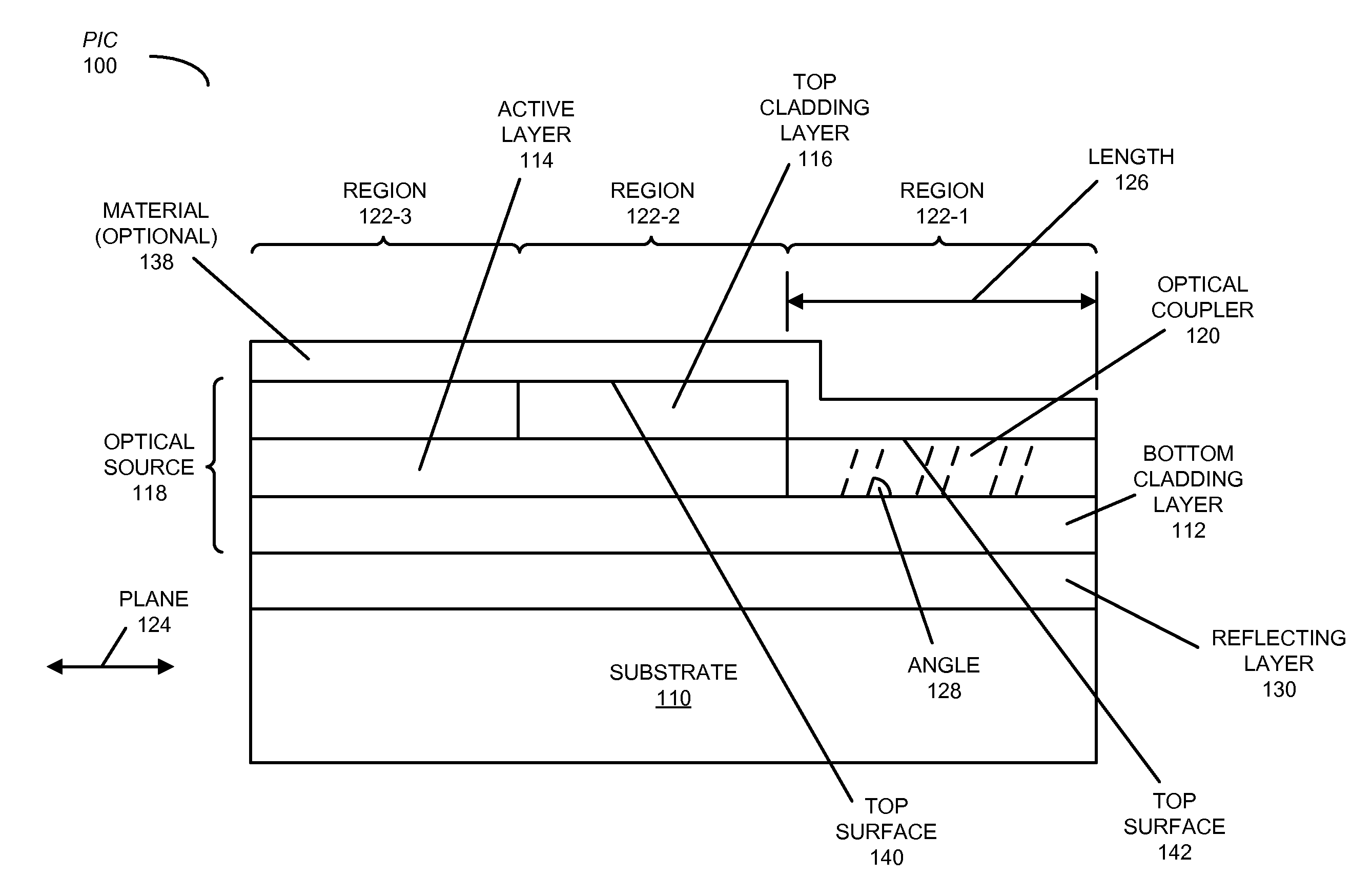
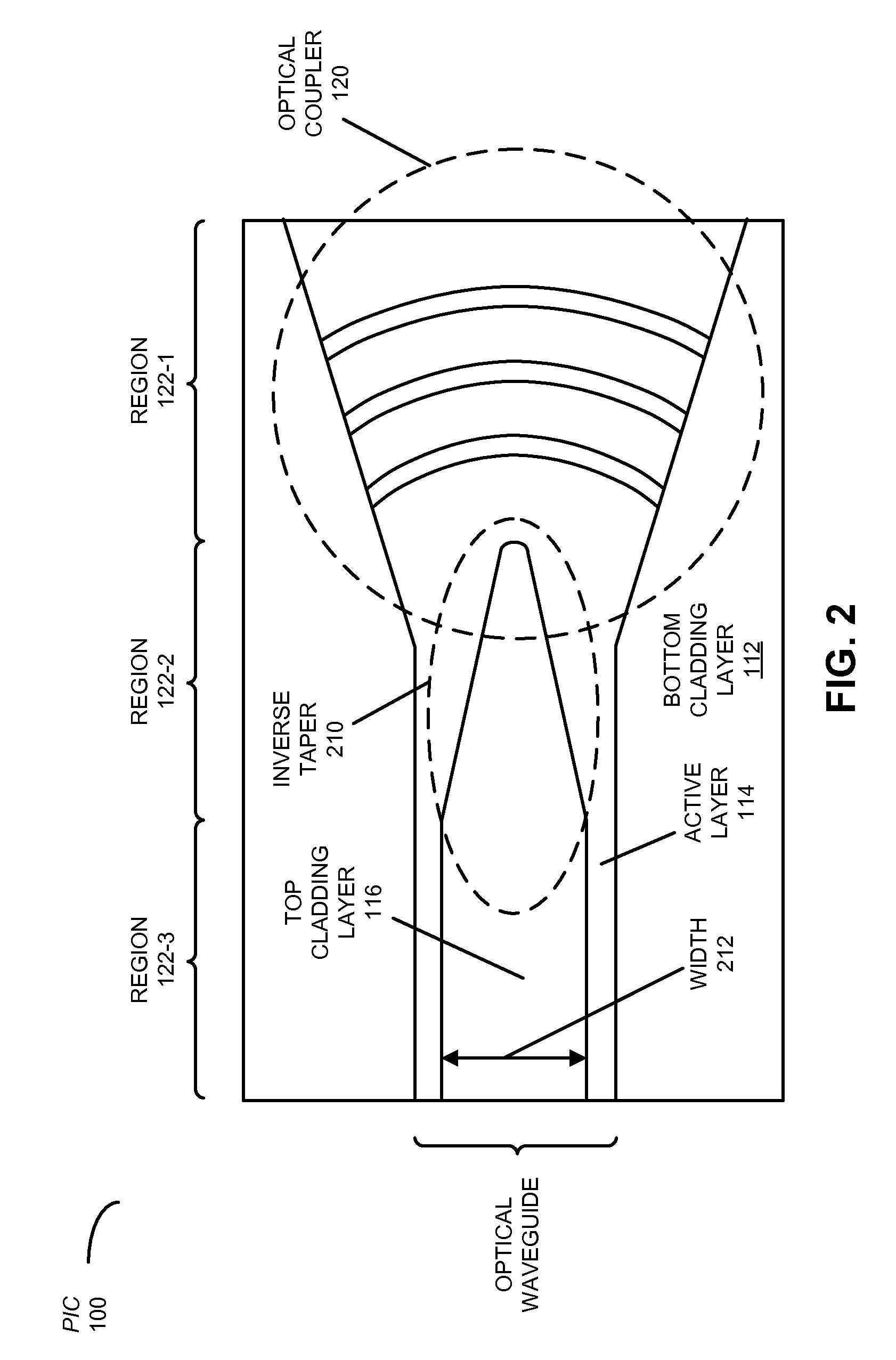
[0026]Embodiments of a photonic integrated circuit (PIC), a system that includes the PIC, and a method for providing an optical signal having a wavelength using the system are described. This PIC includes an optical source that provides an optical signal having the wavelength. In particular, the optical source includes: a reflecting layer, a bottom cladding layer, an active layer (such as a III-V semiconductor) having a bandgap wavelength that exceeds that of silicon (which has an indirect bandgap of 1.12 eV and, thus, a bandgap wavelength larger than 1110 nm), and a top cladding layer. Moreover, an optical coupler (such as a grating coupler) that couples the optical signal out of a plane of the active layer is included in a region of the active layer. In this region, the top cladding layer is absent. Furthermore, in an adjacent region, the top cladding layer includes an inverse taper so that the top cladding layer is tapered down from a width distal from the region.

[0027]This inver...


PUM


Abstract

A photonic integrated circuit (PIC) that includes an optical source that provides an optical signal having a wavelength is described. This optical source includes a reflecting layer, a bottom cladding layer, an active layer (such as a III-V semiconductor) having a bandgap wavelength that exceeds that of silicon, and a top cladding layer. Moreover, an optical coupler (such as a grating coupler) that couples the optical signal out of a plane of the active layer is included in a region of the active layer. In this region, the top cladding layer is absent. Furthermore, in an adjacent region, the top cladding layer includes an inverse taper so that the top cladding layer is tapered down from a width distal from the region. In conjunction with the optical coupler, the inverse taper may facilitate low-loss optical coupling of the optical signal between the PIC and another PIC.

Description

GOVERNMENT LICENSE RIGHTS[0001]This invention was made with United States government support under Agreement No. HR0011-08-9-0001 awarded by DARPA. The United States government has certain rights in the invention.BACKGROUND[0002]1. Field[0003]The present disclosure generally relates to the design of photonic integrated circuits (PICs). More specifically, the present disclosure relates to a PIC that includes a grating coupler that couples an optical signal to another PIC.[0004]2. Related Art[0005]Optical interconnects or links based on silicon photonics have the potential to alleviate inter-chip communication bottlenecks in high-performance computing systems that include multiple processor chips and memory chips. This is because, relative to electrical interconnects, optical interconnects offer significantly improved: bandwidth, density, power consumption, latency, and range.[0006]In order to make a very low power (for example, less than 1 pJ / bit) optical interconnect, a high-efficie...

Claims


Application Information

Patent Timeline
17 Sep 2015
Publication
US20150260913A1
IPC
G02B6/124; G02B6/134; G02B6/34; G02B6/122
CPC
G02B6/124; G02B6/1228; G02B6/4296; G02B6/34; G02B2006/12188; G02B6/1347; G02B6/12004; H01S5/026
Inventors
LI, GUOLIANG; LUO, YING L.