Trench mos semiconductor device

a semiconductor device and trench technology, applied in the direction of semiconductor devices, basic electric elements, electrical equipment, etc., can solve the problems of increasing the switching loss, difficult to increase a dielectric strength, and the field concentration in the bottom portion of the trenches 104/b> is liable to increase, so as to prevent a malfunction of an overcurrent protection circuit, and reduce the feedback capacitance

Active Publication Date: 2015-09-24
FUJI ELECTRIC CO LTD
View PDF4 Cites 22 Cited by
  • Summary
  • Abstract
  • Description
  • Claims
  • Application Information

AI Technical Summary

Benefits of technology

[0027]As the trench MOS semiconductor device, an insulated gate bipolar transistor or a field effect transistor can be used.
[0028]By adopting the previously described configuration, the feedback capacitance of a sense IGBT decreases when an IGBT is turned on, meaning that the sense IGBT is turned on prior to a main IGBT. Also, structurally, as the area wherein a semiconductor substrate is in contact with a gate electrode via an oxide film is reduced, a p-type channel region is provided all over in the semico

Problems solved by technology

Moreover, when the floating region 102-2 is provided, field concentration in the bottom portions of the trenches 104 is liable to increase, meaning that there is also the problem of it being difficult to increase a dielectric strength.
When the gate capacitance increases, there arises the problem that the time required for charging and discharging is lengthened, thus increasing the switching loss.
Because of this, it may happen that

Method used


Image

  • Trench mos semiconductor device
  • Trench mos semiconductor device
  • Trench mos semiconductor device

Examples


first embodiment

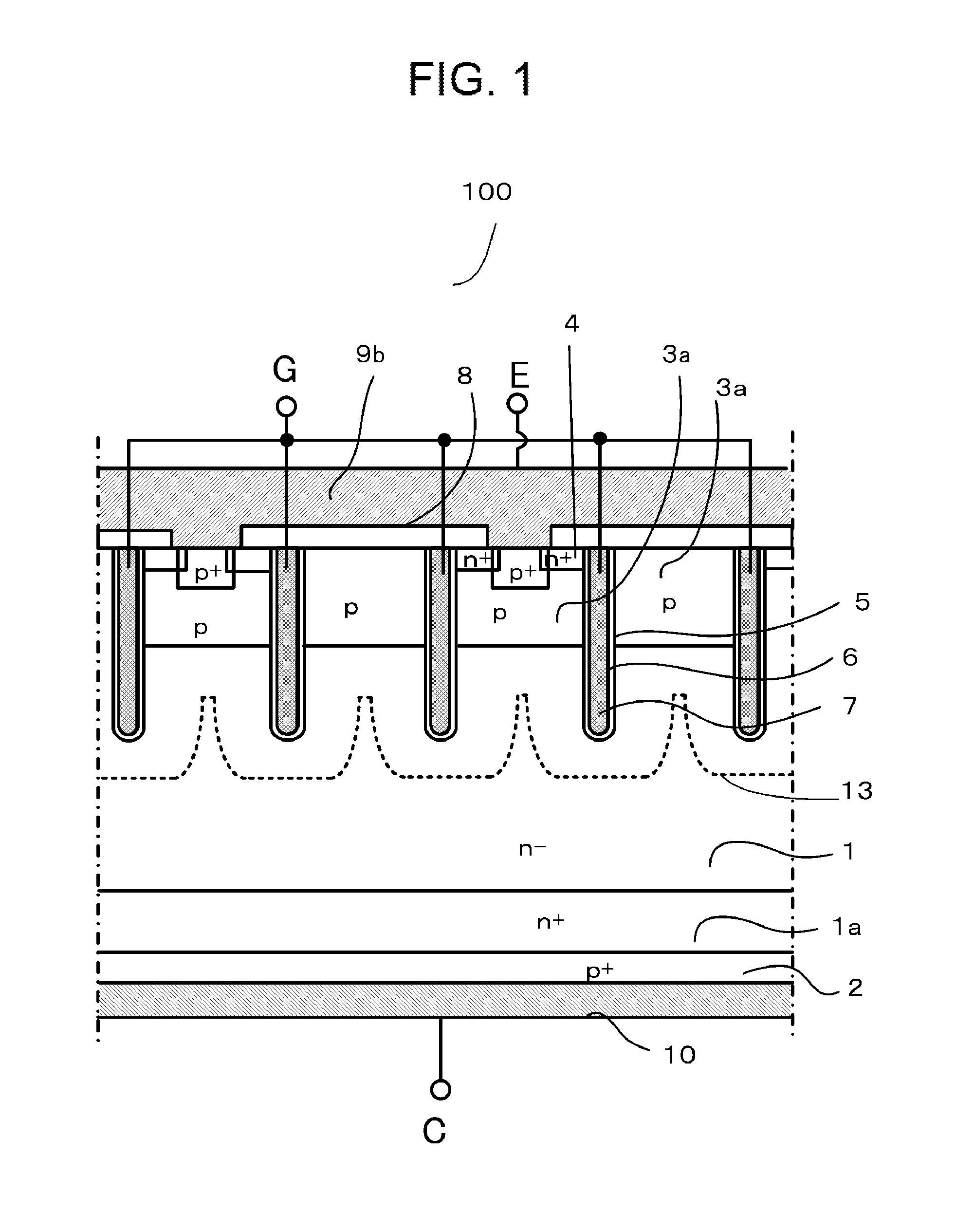
[0042]FIG. 9 shows an equivalent circuit of an IGBT 20 according to the invention used in combination with an overcurrent protection circuit 30. The IGBT 20 in FIG. 9 is such that a main IGBT 21 and a current detection sense IGBT 22 connected in parallel to the main IGBT 21 are formed in an identical semiconductor substrate. A sense current Isense (Is) flowing through the sense IGBT 22 is a minute current corresponding to the area ratio of the active region of the sense IGBT 22 to the active region of the main IGBT 21, relative to a main current Imein (Im) flowing through the main IGBT 21. The term “the active region” here is a region, located in the central portion of a semiconductor substrate chip of the IGBT and surrounded by an edge region on the periphery of the chip, which secures the reliability of dielectric strength and through which the main current flows. Furthermore, when the main and sense IGBTs are turned on, in addition to the sense current Is, a displacement current ...

second embodiment

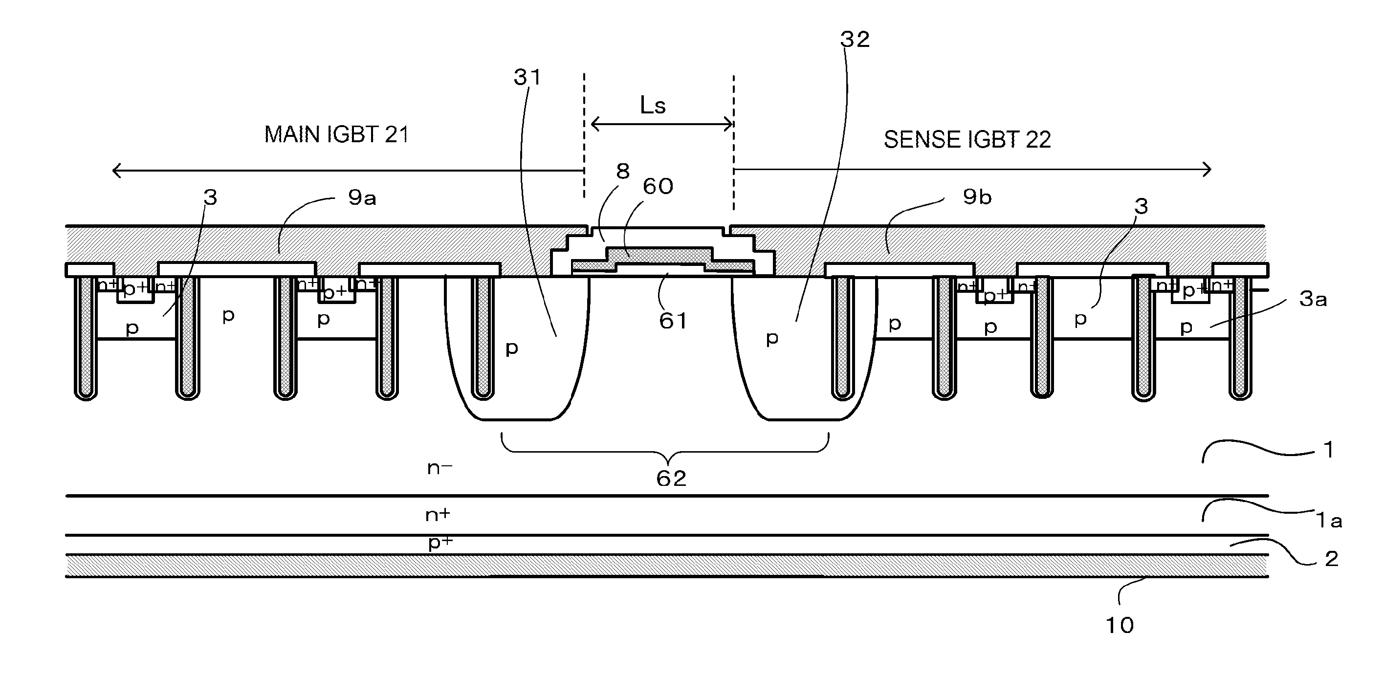
[0063]A description will be given, referring to FIG. 11, of a separating structure or space portion 62 of the main IGBT 21 and sense IGBT 22. Consideration will be given to a case in which the main IGBT 21 and the sense IGBT 22 are continuously formed without particularly providing the separating structure 62 (having a separation interval Ls). At this time, as the n−-type drift layers 1 of the main IGBT 21 and sense IGBT 22 are electrically connected together via the internal resistors of the p-type channel regions 3a, it is unavoidable for a current to leak from one IGBT to the other. Meanwhile, consideration will be given to a case in which the sense IGBT 22 and the main IGBT 21 are spaced from each other, and the separation interval Ls is provided therebetween. At this time, the narrower the separation interval Ls is made, a current flowing through the sense IGBT shifts away from a current ratio corresponding to the area ratio of the sense IGBT to the main IGBT, meaning that curr...


PUM


Abstract

To prevent a malfunction of an overcurrent protection circuit without increasing an on-voltage, and to suppress a short circuit capacity, thus further reducing a switching loss, a trench gate IGBT is provided in which is incorporated a sense IGBT connected in parallel to a main IGBT, where only the sense IGBT portion includes a p-type channel region all over in a semiconductor substrate between adjacent parallel striped trenches, so that the capacitance of the MOS gate of the sense IGBT is smaller than the capacitance of the MOS gate of the main IGBT.

Description

CROSS-REFERENCE TO RELATED APPLICATIONS[0001]This application claims priority from Japanese Patent Application JP 2014-055728, filed on Mar. 19, 2014, hereby incorporated by reference.BACKGROUND OF THE INVENTION[0002]1. Field of the Invention[0003]The present invention relates to a trench MOS semiconductor device mounted on a power conversion device such as an inverter.[0004]2. Description of the Background Art[0005]A power MOS semiconductor device includes main electrodes provided one on each surface in order to cause a main current to flow in a vertical direction (a thickness direction) of a semiconductor substrate and a gate electrode for on / off controlling the main current on one surface side. An insulated gate bipolar transistor (hereafter abbreviated to an IGBT) or a MOS field effect transistor (MOSFET) is a typical device thereof. A power MOS semiconductor device such as the IGBT has a unit cell aggregate structure in which a large number of unit cells each including the laye...

Claims


Application Information

Patent Timeline
IPC IPC(8): H01L29/78H01L29/06H01L29/08H01L29/739
CPCH01L29/7815H01L29/7397H01L29/7813H01L29/0804H01L29/0696H01L29/0619H01L29/402H01L2224/0603
Inventor KUMADA, KEISHIROU
Owner FUJI ELECTRIC CO LTD
Why Eureka
Try Eureka