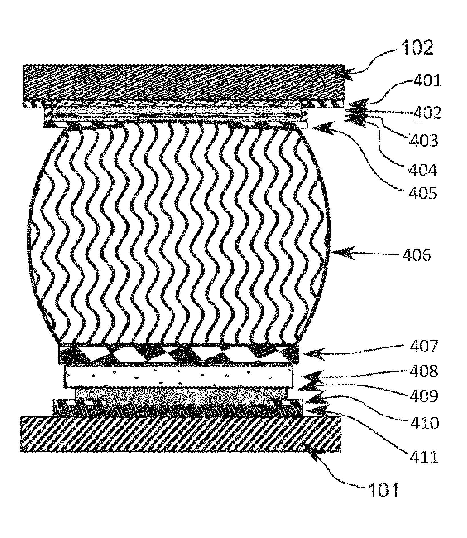
Semiconductor bump-bonded x-ray imaging device
a bump-bonded x-ray and semiconductor technology, applied in the direction of radiation control devices, instruments, x/gamma/cosmic radiation measurement, etc., to achieve the effect of reliable manufacturing
- Summary
- Abstract
- Description
- Claims
- Application Information
AI Technical Summary
Benefits of technology
Problems solved by technology
Method used
Image
Examples
Embodiment Construction
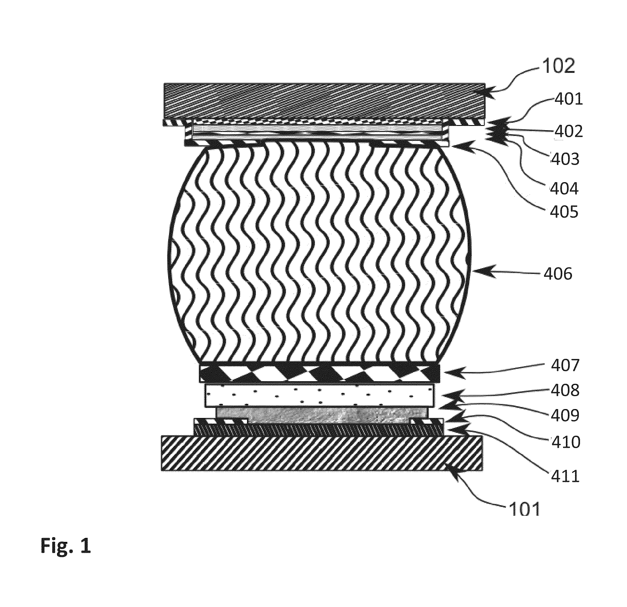
[0020]With reference to FIG. 1, an imaging device, which can be made using previously known technology, is shown where a CMOS pixel 101 is bump-bonded to the corresponding detector pixel 102 via bump 406. A bump 406 is seen on a semiconductor readout pixel 101 (e.g., a CMOS). The bump 406 is of spherical shape. Under the bump one or more seed metal layers have been deposited. Typically, the seed layers are grown on the CMOS readout wafer 101 via sputtering or evaporation technique. Such a bump-bonded imaging device is shown in FIG. 1 and Table 1 all the elements are described with like numbers in the table below, indicating also the average thickness:
TABLE 1Thickness (μm)NameNumberMaterial(example average)Detector pad401Pt (Platinum)0.050UBM 1402Au (Gold)0.030UBM 2403Ni (Nickel)0.050UBM 3404Au (Gold)0.080Detector passivation405AlN0.150(AluminumNitride)Bump solder406SnBi10.000(Tin Bismuth)Bump pedestal407Ni (Nickel)1.600Bump seed bulk408Cu (Copper)0.500Bump seed adhesion409TiW0.040(T...
PUM
 Abstract
Description
Claims
Application Information


