Lithography illumination system

Active Publication Date: 2015-10-08
SHANGHAI INST OF OPTICS & FINE MECHANICS CHINESE ACAD OF SCI
View PDF3 Cites 6 Cited by
  • Summary
  • Abstract
  • Description
  • Claims
  • Application Information

AI Technical Summary

Benefits of technology

The present invention provides a lithography illumination system with improved performance by reducing the scanning distance and speed of the scanning slit, improving transparency, and achieving non-polarized illumination. The system uses a micro-integrator rod array as the homogenizer, eliminating the need for a large illumination lens group and reducing absorption loss. The micro-scanning slit array also reduces the influence of vibration and improves system performance. This invention has a simple structure and is highly efficient.

Problems solved by technology

So the performance of the illumination system may directly affect the performance of the lithography tool.
The illumination lens group 8 generally has large aperture (nearly 300 mm) and many lenses (10 pieces or so), which reduces the system's transmittance, reduce energy usage ratio, and makes the structure complex.

Method used


Image

  • Lithography illumination system
  • Lithography illumination system
  • Lithography illumination system

Examples


Embodiment Construction

[0021]The present invention is further illustrated in the example and drawings, but the scope of protection should not be limited to the examples.

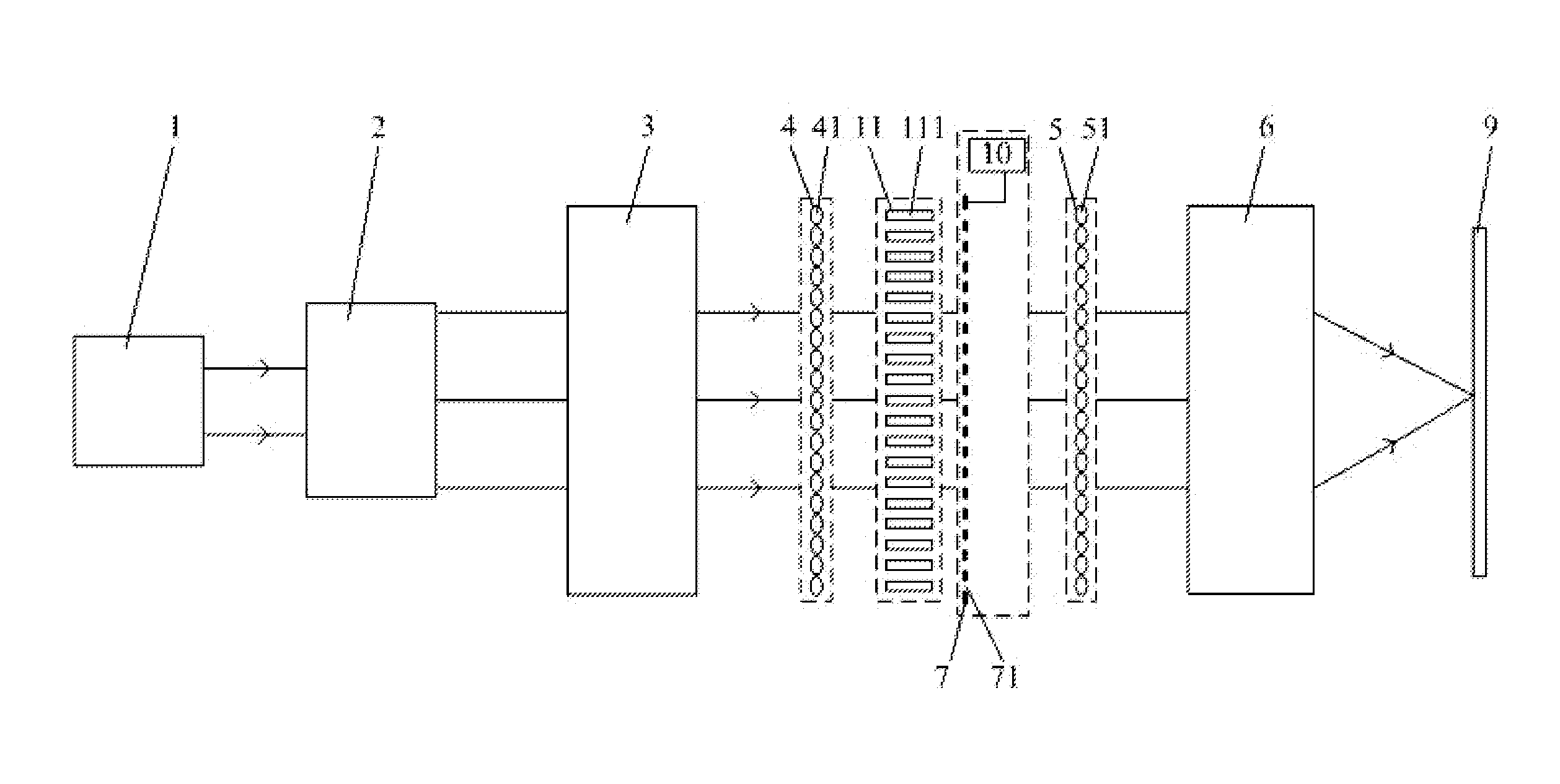
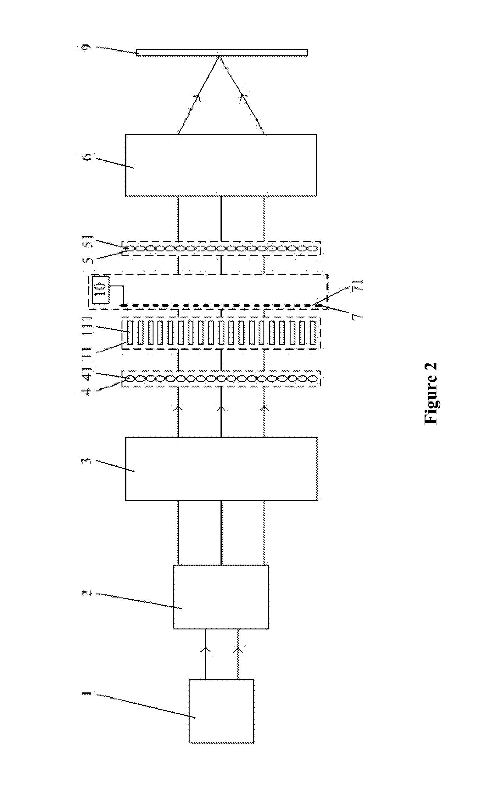
[0022]As shown in FIG. 2, the lithography illumination system of the present invention comprises a laser light source 1, a collimating and expanding unit 2, a pupil shaping unit 3, a first micro-lens array 4, a second micro-lens array 5, a condenser lens group 6, a micro-scanning slit array 7, a mask 9, a motion control unit 10, and a micro-integrator rod array 11. The components are spatially arranged as follows: a beam emitted from the laser light source 1 sequentially passes through the collimating and expanding unit 2, the pupil shaping unit 3, the first micro-lens array 4, the micro-integrator rod array 11, the micro-scanning slit array 7, the second micro-lens array 5, and the condenser lens group 6, and then, illuminates the mask 9; the motion control unit 10 is connected to the micro-scanning slit array 7 for controlling the moving...


PUM


Abstract

A lithography illumination system, along the transmission direction of the laser light, successively comprising a laser light source, a collimating and expanding unit, a pupil shaping unit, a first micro-lens array, a micro-integrator rod array, a micro-scanning slit array, a second micro-lens array, a condenser lens group, a mask, and and a motion control unit for controlling the motion of the micro scanning slit array.

Description

CROSS-REFERENCE AND RELATED APPLICATIONS[0001]The subject application is a continuation-in-part of PCT international application PCT / CN2013 / 000493 filed on Apr. 28, 2013, which in turn claims priority on Chinese patent application CN 201310030574.9 filed on Jan. 25, 2013. The contents and subject matters of all the priority applications are incorporated herein by reference.TECHNICAL FIELD[0002]The present invention relates to the field of lithography techniques, particularly, a lithography illumination system.BACKGROUND OF THE INVENTION[0003]With rapid development of the microelectronics industry, the research and development of high-end scanning lithography tool for manufacturing large scale integrated circuit has become an urgent demand. The illumination system may provide high illumination uniformity, control exposure dose, and implement off-axis illumination for the lithography tool to improve the resolution and increase the depth of the focus, and it is an important part of the...

Claims


Application Information

Patent Timeline
IPC IPC(8): G03F7/20G02B19/00G02B26/10G02B3/00
CPCG03F7/7015G02B26/101G02B19/0047G02B3/0037G03F7/70066G03F7/70075
Inventor ZENG, AIJUNZHU, LINGLINFANG, RUIFANGHUANG, HUIJIE
Owner SHANGHAI INST OF OPTICS & FINE MECHANICS CHINESE ACAD OF SCI
Why Eureka
Try Eureka