
Method for fabrication of copper-indium gallium oxide and chalcogenide thin films

a technology of copper-indium gallium oxide and chalcogenide, which is applied in the direction of chemistry apparatus and processes, sustainable manufacturing/processing, and final product manufacturing, etc., can solve the problems of high capital expense and vacuum processing of the deposition method of chalcogenid

Inactive Publication Date: 2015-10-15
THE UNITED STATES OF AMERICA AS REPRESENTED BY THE SECRETARY OF THE NAVY
View PDF2 Cites 6 Cited by
  • Summary
  • Abstract
  • Description
  • Claims
  • Application Information

AI Technical Summary

Benefits of technology

The present invention provides a way to make CIGS absorber layers using a simple and cheap method. This method uses nanoparticles that are easy to make and can be deposited layer by layer using a process that doesn't require a vacuum. This method is compatible with high throughput manufacturing and uses readily available precursors. Compared to other methods, this invention offers a more scalable and cost-effective solution for making CIGS absorber layers.

Problems solved by technology

Other CIGS deposition methods rely on vacuum processing (high capital expense) or on nanoparticle solutions or metallic inks that use hazardous solvents and are difficult to produce.

Method used


Image

  • Method for fabrication of copper-indium gallium oxide and chalcogenide thin films
  • Method for fabrication of copper-indium gallium oxide and chalcogenide thin films
  • Method for fabrication of copper-indium gallium oxide and chalcogenide thin films

Examples


Embodiment Construction

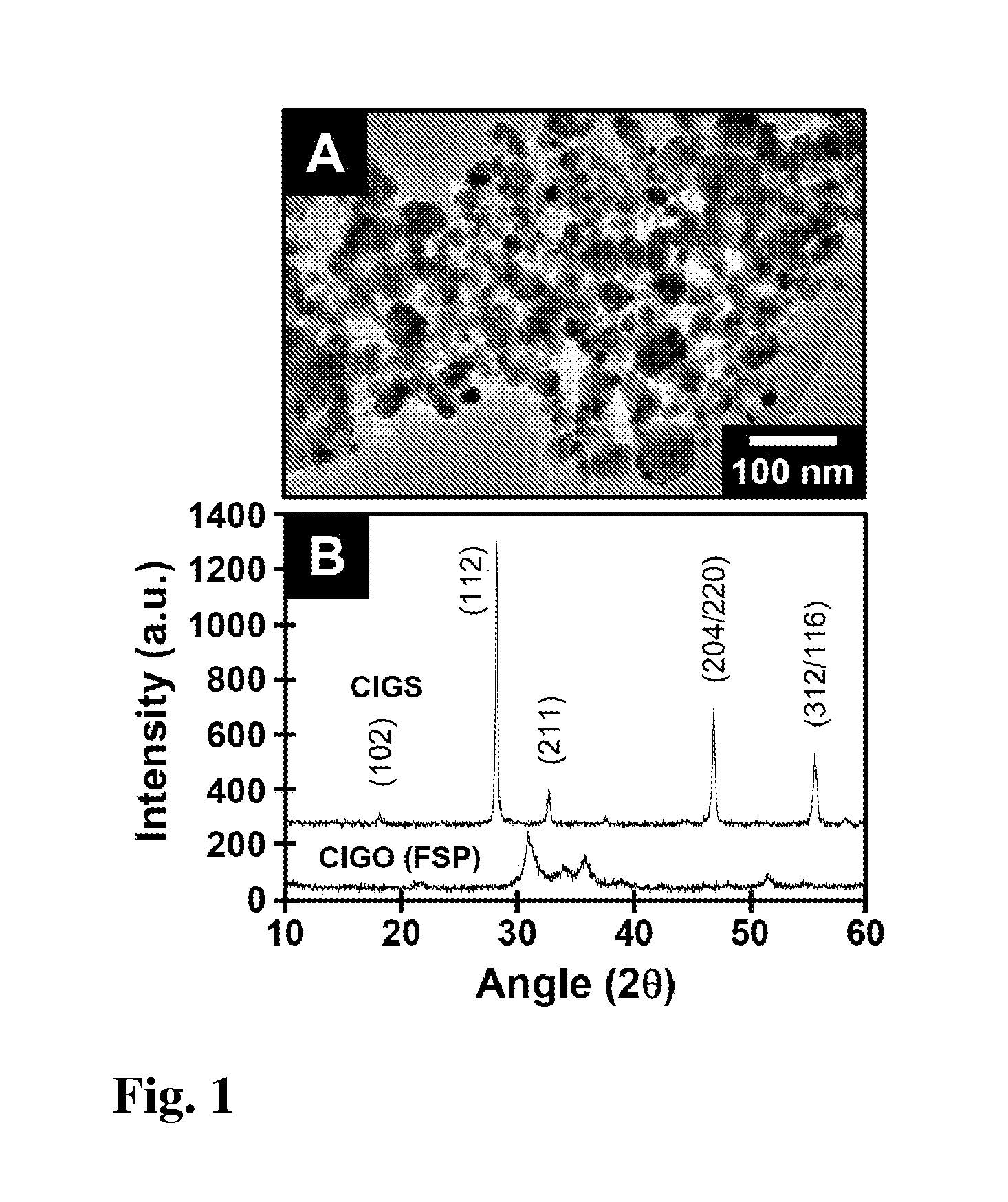
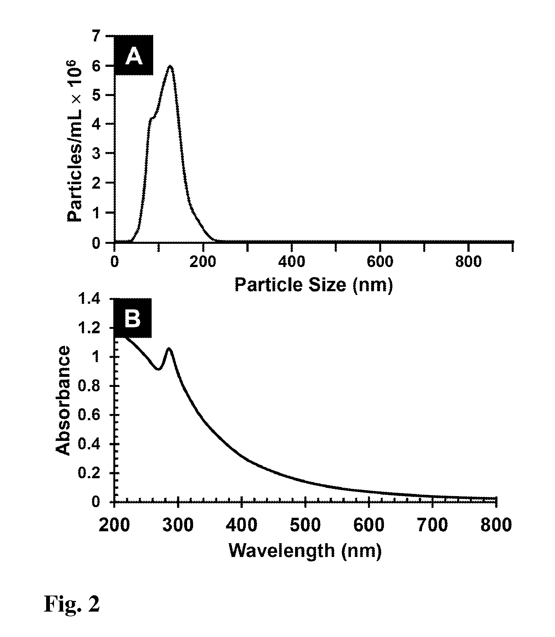
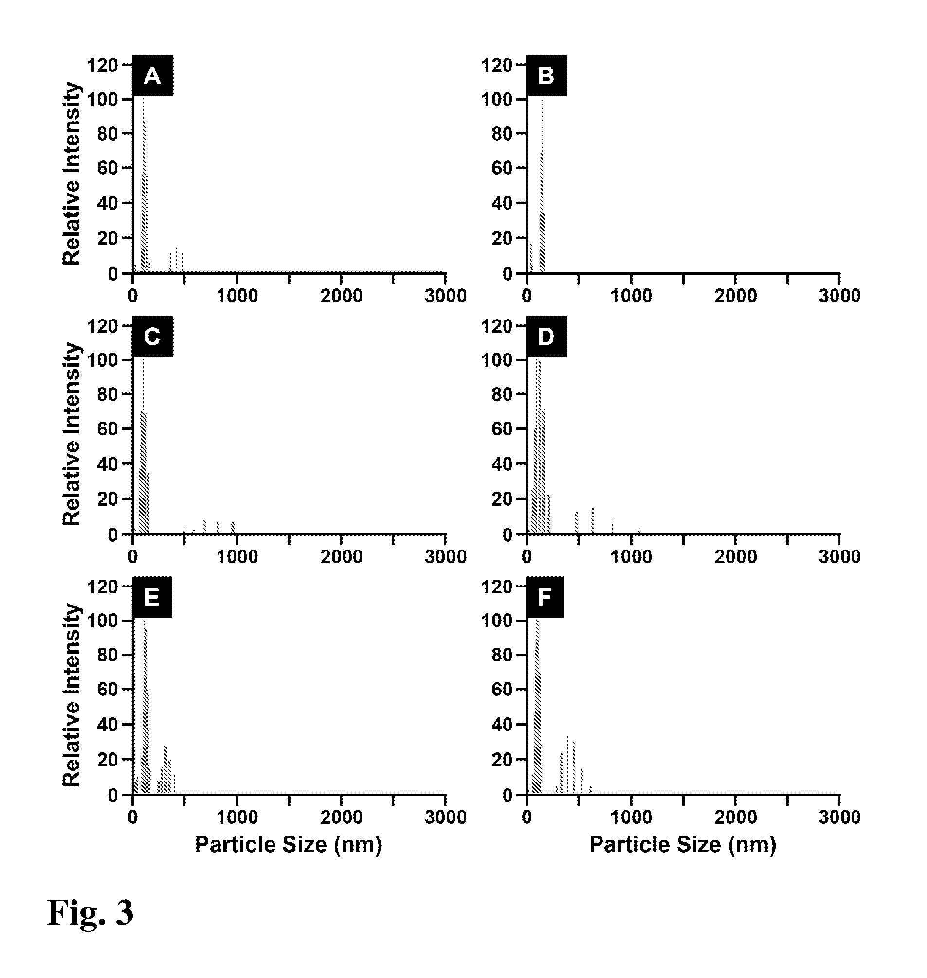
[0023]The present invention provides a unique approach using copper-indium-gallium oxide (CIGO) nanoparticles, which are readily produced in large quantities, in combination with automatable LbL deposition methods for the low cost manufacture of copper-indium-gallium oxide (CIGO) and copper-indium-gallium chalcogenide (such as copper-indium-gallium sulfide (CIGS), copper-indium-gallium selenide (CIGSe), and copper-indium-gallium telluride) films. This method involves gram scale preparations of CIGO nanoparticles using a flame spray pyrolysis (FSP) technique, their subsequent surface modification via binding of polyallylamine (PAH), and the formation of stable aqueous dispersions prepared from the resulting CIGO-PAH colloids. Composite multilayer films comprising the CIGO-PAH colloids, together with polystyrenesulfonate (PSS) or polydopamine (PDA), are further prepared via an aqueous LbL approach and characterized. Subsequent oxidation to remove the organic components and sulfurizati...


PUM

PropertyMeasurementUnit
diameteraaaaaaaaaa
pHaaaaaaaaaa
thicknessaaaaaaaaaa

Abstract

A composition of matter and method of forming copper indium gallium sulfide (CIGS), copper indium gallium selenide (CIGSe), or copper indium gallium telluride thin film via conversion of layer-by-layer (LbL) assembled Cu—In—Ga oxide (CIGO) nanoparticles and polyelectrolytes. CIGO nanoparticles are created via a flame-spray pyrolysis method using metal nitrate precursors, subsequently coated with polyallylamine (PAH), and dispersed in aqueous solution. Multilayer films are assembled by alternately dipping a substrate into a solution of either polydopamine (PDA) or polystyrenesulfonate (PSS) and then in the CIGO-PAH dispersion to fabricate films as thick as 1-2 microns. After LbL deposition, films are oxidized to remove polymer and sulfurized, selenized, or tellurinized to convert CIGO to CIGS, CIGSe, or copper indium gallium telluride.

Description

PRIORITY CLAIM[0001]The present application is a non-provisional application claiming the benefit of U.S. Provisional Application No. 61 / 977,206, filed on Apr. 9, 2014 by Walter J. Dressick et al., entitled “METHOD FOR FABRICATION OF COPPER-INDIUM GALLIUM OXIDE AND CHALCOGENIDE THIN FILMS,” the entire contents of which is incorporated herein by reference.BACKGROUND OF THE INVENTION[0002]1. Field of the Invention[0003]The present invention relates to depositing copper-indium-gallium chalcogenide films using aqueous solutions of precursors.[0004]1. Description of the Prior Art[0005]Quaternary chalcogenide semiconductors of structure CuAxB1-xZ2 (where A, B=In, Ga or Zn, Sn; Z=S, Se, or Te; 0≦x≦1) are among the leading materials candidates under study as absorber layers for conversion of visible and near infrared solar radiation into electricity in photovoltaic devices. These materials offer several important advantages, including composition tunable band gaps for light absorption match...

Claims


Application Information

Patent Timeline
Patent Type & Authority Applications(United States)
IPC IPC(8): H01L31/032H01L31/18B01J6/00H01L31/0352
CPCH01L31/0322B01J6/008H01L31/18H01L31/0352H01L21/02565H01L21/02568H01L21/02601H01L21/02614H01L21/02628Y02E10/541Y02P70/50
Inventor DRESSICK, WALTER J.SANGHERA, JASBINDER S.KIM, WOOHONGBAKER, COLIN C.MYERS, JASON D.FRANTZ, JESSE A.
Owner THE UNITED STATES OF AMERICA AS REPRESENTED BY THE SECRETARY OF THE NAVY
Learn More