Linear image sensor and driving method therefor

a technology of image sensor and driving method, which is applied in the field of linear image sensor, can solve the problems of insufficient signal sn ratio, inability to obtain the correct value of signal, and difficulty in operation, so as to shorten the charge accumulation time, high sn ratio, and long charge accumulation time

Inactive Publication Date: 2015-10-15
SHIMADZU CORP +1
View PDF19 Cites 5 Cited by
  • Summary
  • Abstract
  • Description
  • Claims
  • Application Information

AI Technical Summary

Benefits of technology

[0058]In the linear image sensor and its driving method according to the present invention, it is possible to dramatically shorten the charge accumulation time in an arbitrary number of pixels located at arbitrary positions among the entire group of N pixels as compared to the other pixels. Therefore, when the linear image sensor according to the present invention is used as a detector for a spectrometric device, even if the wavelength-intensity distribution of the light source includes a bright line or similar wavelength at which the light intensity is extremely high as compared to the other wavelength regions, it is possible to prevent one or more pixels receiving the bright line from being saturated with photocharges, while ensuring an adequately long charge accumulation time at any pixel receiving low-intensity light so that the amount of accumulated signals will be close to the saturation level. As a result, high SN ratios can assuredly be achieved at all the pixels without causing signal saturation.

Problems solved by technology

However, having the readout period thus being equal to the charge accumulation time may cause a problem.
If the readout period is always equal to the charge accumulation time, the photodiode will be saturated with accumulated charges when the light intensity is high, making it impossible to obtain the correct value of the signal.
However, this causes the problem that the SN ratio of the signal will be insufficient when the light intensity is low.
However, due to hardware restrictions, such an operation is actually difficult; for example, the readout period is limited by the frequency response of the sensor, and the frequency characteristics of the readout circuit external to the sensor cannot be easily changed.
Decreasing the readout period is particularly difficult.
However, with the technique described in the aforementioned Patent Literature 1, although it is possible to set a charge accumulation time extremely shorter than the readout time T for all the pixels, it is impossible to set a different charge accumulation time for each horizontal line or for each pixel.
Therefore, while it is possible to set an extremely short charge accumulation time common to all the pixels to prevent saturation at the pixels which receive bright lines, this setting prevents the other pixels which do not receive any bright line from producing sufficient amounts of charges, thus causing a deterioration in the SN ratio of the signal.
Although this method allows the setting of a charge accumulation time longer than the readout period at an arbitrary pixel, it does not allow the opposite, i.e. the setting of a charge accumulation time shorter than the readout period at an arbitrary pixel.
Therefore, while the charge accumulation time at pixels which do not receive bright lines can be exclusively increased to ensure adequate amounts of charges at all the pixels, it is difficult to avoid saturation of the pixels receiving the bright lines since the charge accumulation time cannot be shorter than the readout period.
However, directly shortening the readout period is impractical due to the earlier mentioned hardware restrictions.

Method used


Image

  • Linear image sensor and driving method therefor
  • Linear image sensor and driving method therefor
  • Linear image sensor and driving method therefor

Examples


first embodiment

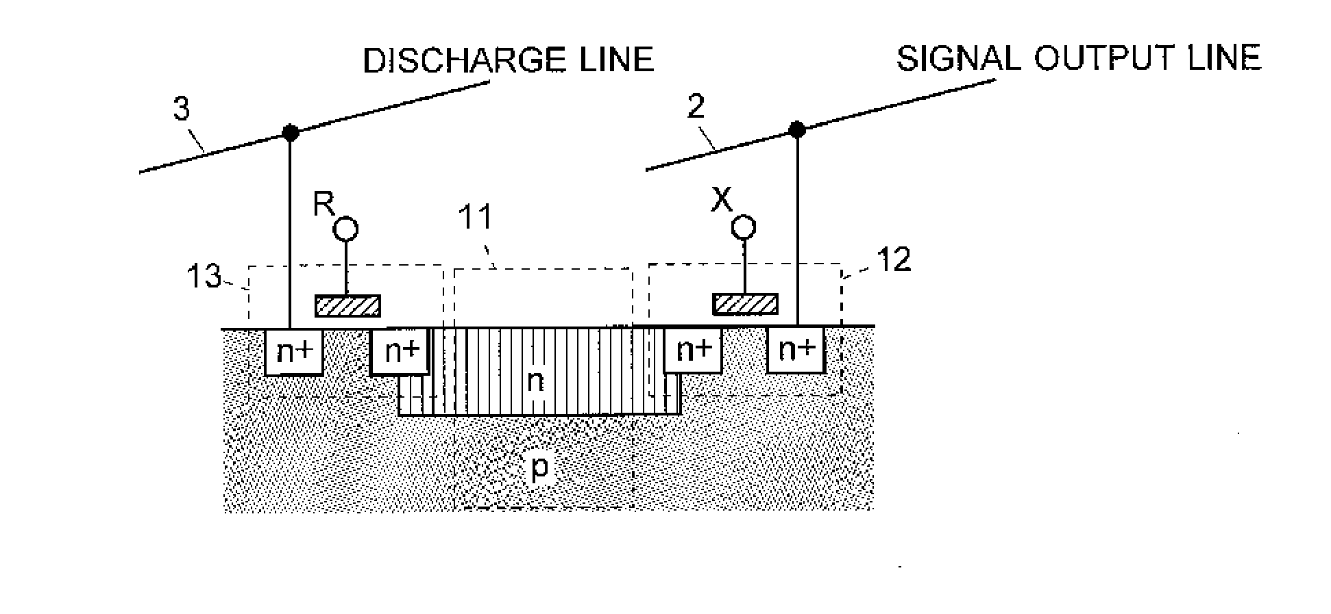
[0068]An embodiment (first embodiment) of the linear image sensor and its driving method according to the present invention is hereinafter described with reference to the attached drawings.

[0069]The linear image sensor of the first embodiment (and that of the second embodiment, which will be described later) is suitable as a detector for a spectrophotometer as shown in FIG. 4. Measurement light emitted from the bright point in a light source 100 having a specific emission spectrum (e.g. a deuterium lamp, tungsten lamp or xenon lamp) is focused by a lens 101 and cast into a sample cell 103 made of quartz glass or a similar transparent material with a liquid sample 104 held inside. After passing through the liquid sample 104, the transmitted light is focused by a lens 105 and falls onto a light-dispersing device 107 (e.g. a diffraction grating) through a slit 106. The transmitted light is dispersed into wavelengths in a one-dimensional direction by the light-dispersing device 107. The...

second embodiment

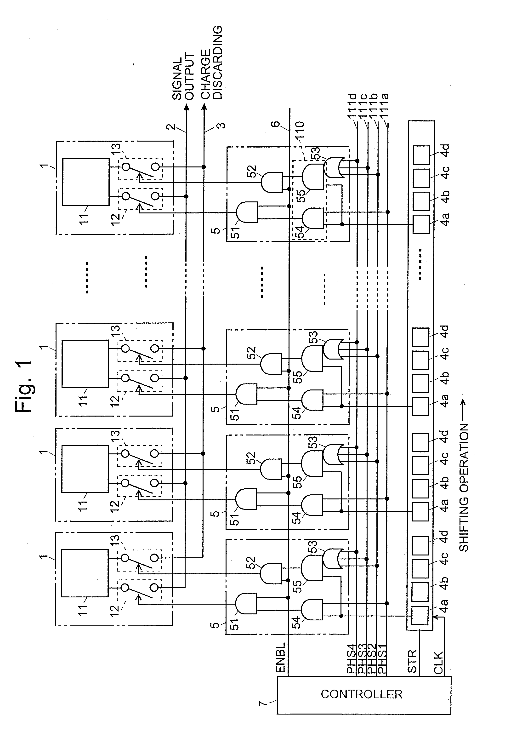
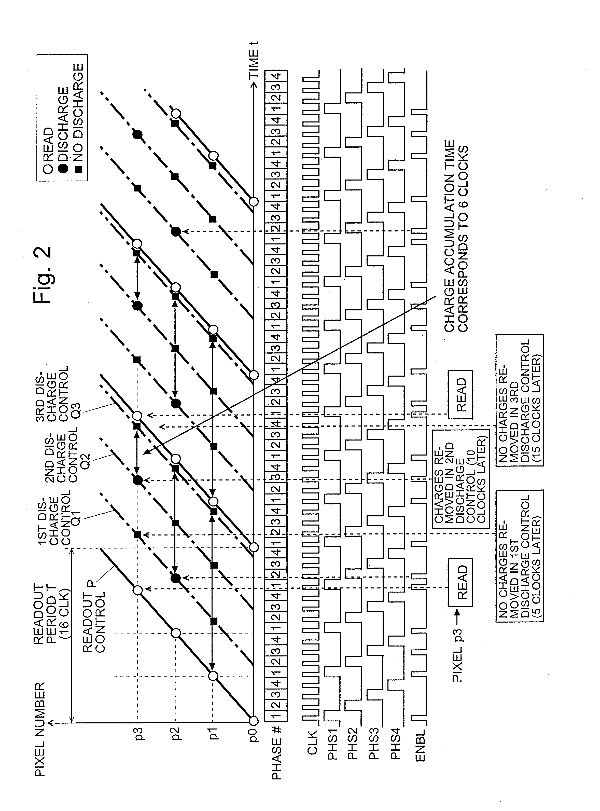
[0091]A linear image sensor and its driving method according to the second embodiment different from the first embodiment is hereinafter described using FIGS. 5 and 6. FIG. 5 is a configuration diagram showing the main components of the linear image sensor according to the second embodiment, and FIG. 6 is a model diagram illustrating the driving method for controlling the charge accumulation time in the linear image sensor of the second embodiment. The components identical or corresponding to those of the first embodiment are denoted by the same numerals.

[0092]The linear image sensor of the second embodiment is completely identical to that of the first embodiment in terms of the configuration of each individual pixel 1. A difference exists in that the number of shift registers is increased in exchange for the decreased number of stages of each shift register. It should be noted that the second embodiment is configured to realize only one choice of the charge accumulation time that i...


PUM


Abstract

A logical gate circuit (5) and four stages of flip flips (4a-4d) are assigned to each pixel (1). A controller (7) inputs four phase identification signals into the logical gate circuit (5) and also inputs a start signal STR into a shift register (4) synchronously with the four mutually different phases defined by the phase identification signals. During one round of scanning all the pixels (1) for a readout control, if an enable signal ENBL is set to “0” while an output of a phase identification circuit (110) is “1”, a charge accumulation time at the pixel (1) concerned becomes equal to a readout period T. If the enable signal ENBL is set to “1” while the output of the phase identification circuit (110) is “1”, electric charges accumulated in a photodiode (11) until that point are entirely discarded, so that the charge accumulation time becomes shorter than the readout period T. Thus, the charge accumulation time at each pixel (1) can be controlled to ensure an adequate SN ratio while avoiding signal saturation at some pixels even if the light source has a bright line at a specific wavelength.

Description

TECHNICAL FIELD[0001]The present invention relates to a linear image sensor consisting of a plurality of photoelectric conversion elements arrayed in a one-dimensional form, as well as a method for driving such a sensor. In particular, it relates to a linear image sensor suitable for detecting light dispersed into wavelengths in a spectrometric device, such as a spectrophotometer or fluorescence analyzer, along with a method for driving such a sensor.BACKGROUND ART[0002]In a spectrometric device, such an ultraviolet-visible spectrophotometer or a spectroscopic detector for a liquid chromatograph, a linear image sensor having a large number (e.g. from 128 to 1024 pieces) of one-dimensionally arrayed photodiodes made of silicon (Si), indium gallium arsenide (InGaAs) or other semiconductors as the base material, is used for simultaneous detection of light dispersed into wavelengths by a light-dispersing device. Linear image sensors are roughly divided into the CCD type and CMOS type. I...

Claims


Application Information

Patent Timeline
Patent Type & Authority Applications(United States)
IPC IPC(8): H04N5/378H04N5/376
CPCH04N5/3765H04N5/378H01L27/14609H04N25/701H04N25/767H04N25/75H04N25/745
Inventor TOMINAGA, HIDEKIHIROSE, RYUTATAKUBO, KENJISUGAWA, SHIGETOSHIKURODA, RIHITO
Owner SHIMADZU CORP
Why Eureka
Try Eureka