Reducing leakage current in semiconductor devices

Active Publication Date: 2015-11-05
MASSACHUSETTS INST OF TECH
View PDF4 Cites 17 Cited by
  • Summary
  • Abstract
  • Description
  • Claims
  • Application Information

AI Technical Summary

Benefits of technology

[0013]Some embodiments relate to a semiconductor device, comprising: a first region comprising a first semiconductor material; a second region comprising a second semiconductor mat

Problems solved by technology

However, the limited critical electric field of silicon and its relatively high resistance causes available commercial devices, circuits and systems to be very large and heavy, and operate at low frequencies.
Therefore, such commercial devices are unsuitable for future generations of hybrid vehicles and other applications.
However, the drawbacks of SiC substrates include a limited available wafer size (up to 4 inches) and high cost.
However, the major drawback of sapphire substrates is their poor thermal conductivity.
In power electronics appl

Method used


Image

  • Reducing leakage current in semiconductor devices
  • Reducing leakage current in semiconductor devices
  • Reducing leakage current in semiconductor devices

Examples


Embodiment Construction

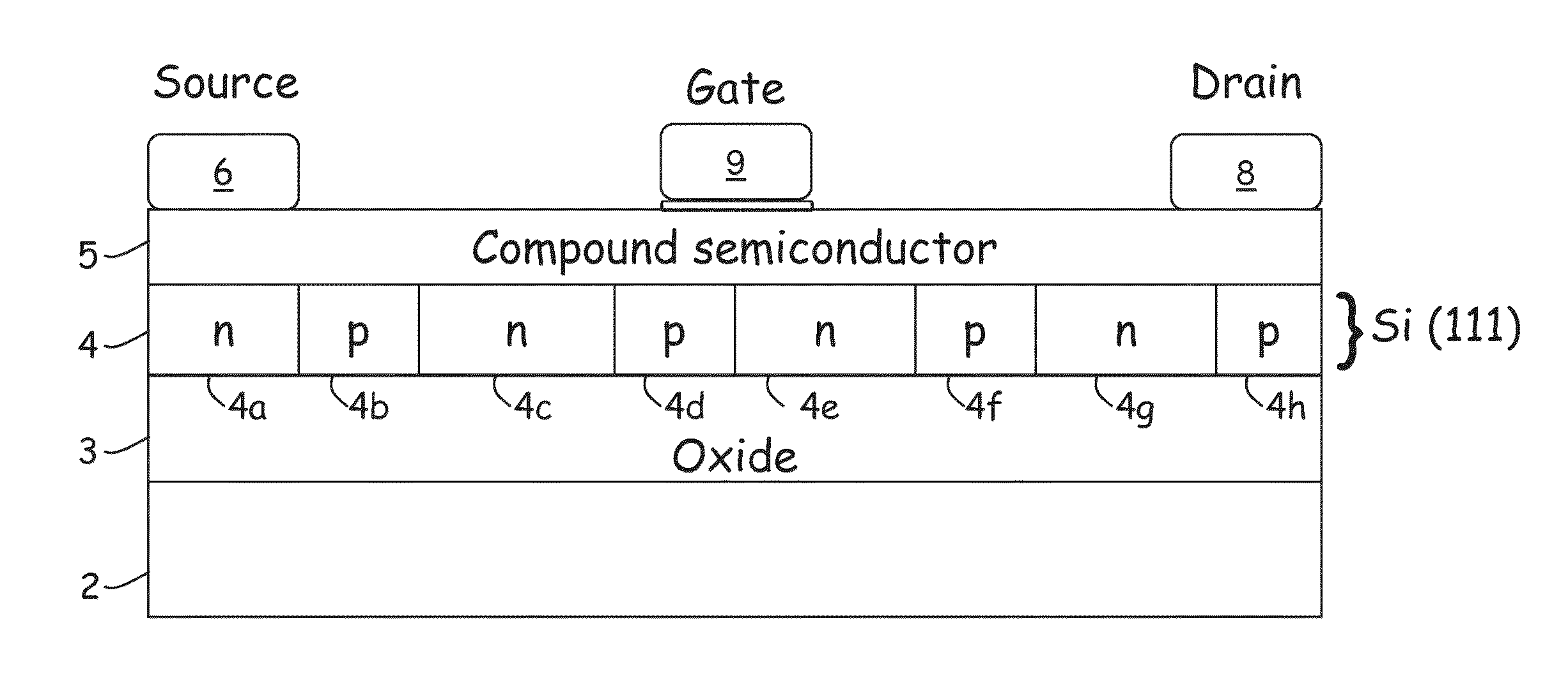
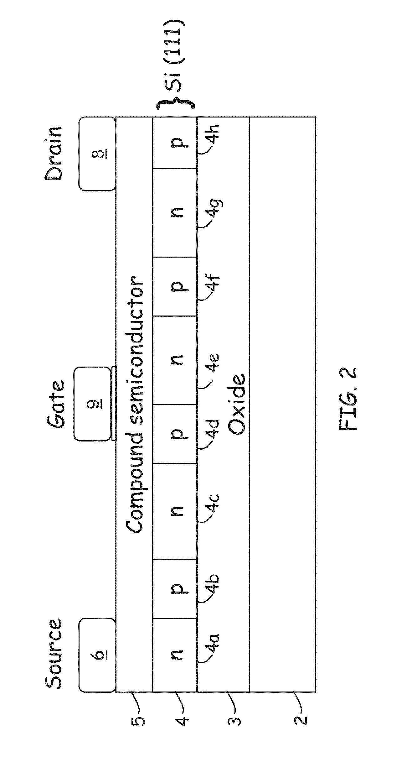
[0029]According to the innovative techniques described herein, a reduction in leakage current and / or an increase in breakdown voltage can be achieved for compound semiconductor based devices, such as nitride semiconductor devices, for example, formed on a substrate that includes a second semiconductor material, such as silicon, for example. In some embodiments, a current blocking structure may be formed in the substrate to reduce and / or prevent the flow of leakage current through the substrate and / or to engineer the electric field at the surface of the substrate. Such techniques can provide improvements in power transistors that will enable significant improvements in systems such as hybrid vehicles, high efficiency power inverters for solar cells, and power converters for LEDs, for example.

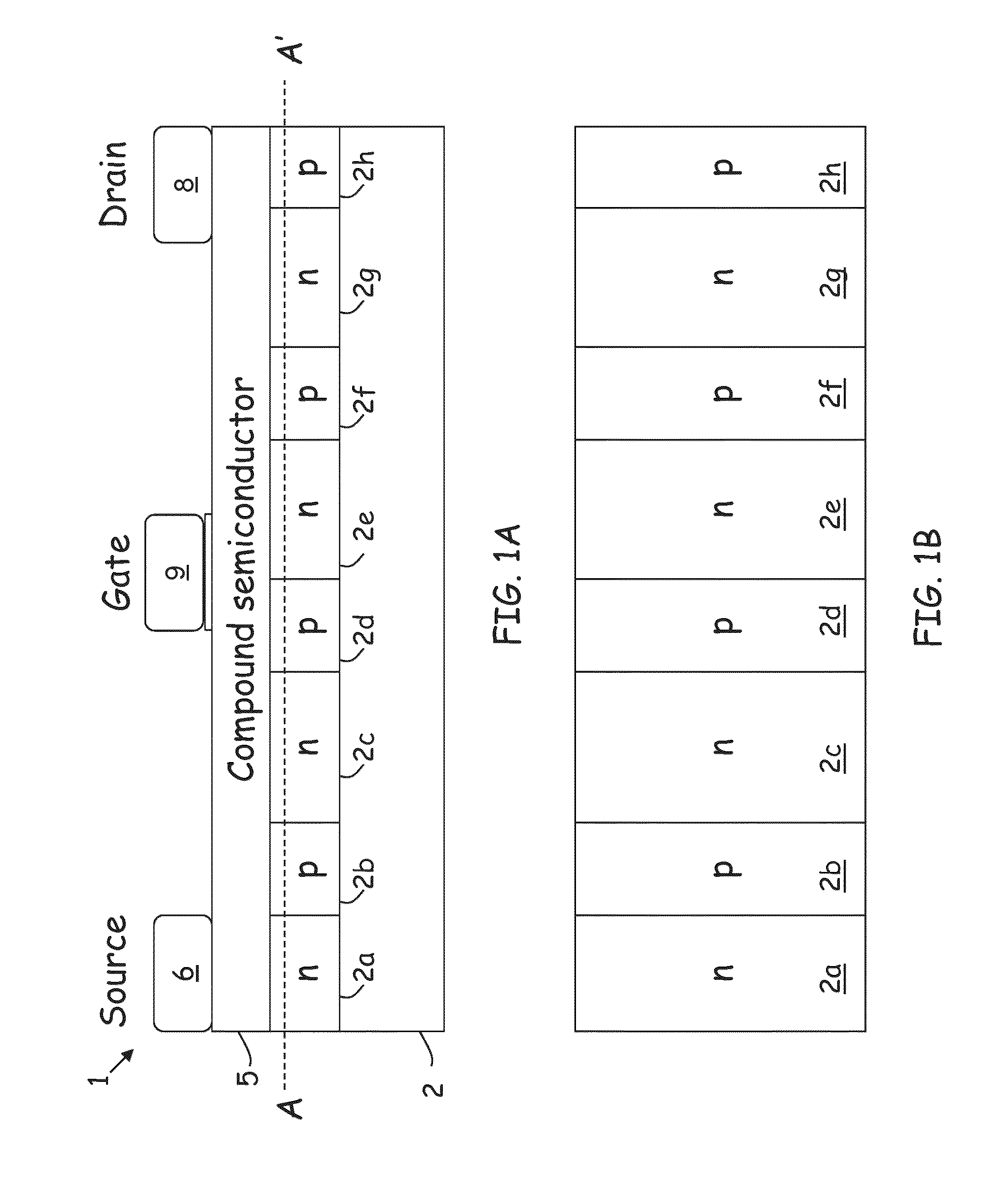
[0030]An embodiment of a semiconductor device 1 having a current blocking structure with p-n junctions is shown in FIGS. 1A and 1B, which show a cross-sectional view and a plan view of a semicond...


PUM


Abstract

A semiconductor device includes a first region having a first semiconductor material and a second region having a second semiconductor material. The second region is formed over the first region. The semiconductor device also includes a current blocking structure formed in the first region between first and second terminals of the semiconductor device. The current blocking structure is configured to reduce current flow in the first region between the first and second terminals.

Description

CROSS-REFERENCE TO RELATED APPLICATIONS[0001]This application claims priority to U.S. provisional application Ser. No. 61 / 735,604, titled “Unconventional Nitride-on-Si Substrate Structures,” filed Dec. 11, 2012, which is hereby incorporated by reference in its entirety.BACKGROUND[0002]1. Field of Invention[0003]The techniques described herein relate to semiconductor devices and methods that can reduce leakage current and increase breakdown voltage for semiconductor devices. Such structures and methods can be used advantageously for devices having a compound semiconductor material such as a III-V semiconductor material, e.g., a III-N semiconductor material, such as GaN (Gallium Nitride), for example, formed over a second semiconductor material, such as silicon, for example.[0004]2. Discussion of the Related Art[0005]Improved power transistors are desired for advanced transportation systems, more robust energy delivery networks and new approaches to high-efficiency electricity generat...

Claims


Application Information

Patent Timeline
IPC IPC(8): H01L29/267H01L21/306H01L29/78H01L29/06H01L29/20H01L21/02H01L29/10
CPCH01L29/267H01L21/02381H01L21/0254H01L21/30604H01L29/78H01L29/1033H01L29/0688H01L29/0649H01L29/2003H01L29/1079H01L21/8258H01L29/7786
Inventor LU, BINMATIOLI, ALISON DE NAZARETHPALACIOS, TOMAS APOSTOL
Owner MASSACHUSETTS INST OF TECH
Why Eureka
Try Eureka