Method for manufacturing soi wafer and soi wafer
- Summary
- Abstract
- Description
- Claims
- Application Information
AI Technical Summary
Benefits of technology
Problems solved by technology
Method used
Image

Examples
example 1
[0055]An SOI wafer was produced by using a Si single crystal wafer of 300 mm in diameter and in crystal orientation. In that occasion, a thermal oxide film of 150 nm was grown on a bond wafer in a heat treat furnace, and hydrogen ions (H+ ions) were ion-implanted into this wafer in dose amount of 5×10¹⁶ / cm2 and with acceleration energy of 40 keV. A base wafer consisting of a Si single crystal wafer was prepared, oxygen plasma treatment was performed only on the base wafer, and thereafter, bonding with the ion-implanted bond wafer was performed. After an annealing at 200° C. for 4 hours as the first step had been performed on this bonded wafer, the temperature was raised at a rate of temperature rise of 10° C. / min, and an annealing at 400° C. for 6 hours as the second step was performed. The wafer was delaminated by this heat treatment and became an initial SOI wafer.
experimental examples
Experimental Example 1
[0065]An experiment that the first step and the second step for wafer separation (delamination) are combined was performed under the following conditions.
[0066]An SOI wafer was produced by using Si single crystal wafers of 300 mm in diameter and in crystal orientation as a bond wafer and a base wafer.
[0067]First, a thermal oxide film of 150 nm was grown on the bond wafer in the heat treat furnace. Hydrogen was ion-implanted into this wafer in dose amount of 5×10¹⁶ / cm2 and with acceleration energy of 40 keV. The base wafer (with no oxide film) was prepared, nitrogen plasma treatment was performed on the base wafer, and thereafter bonding was performed. As delamination heat treatment, 2-hour annealing was performed on this bonded wafer within a range of 150 to 350° C. as the first step, the temperature was raised at 10° C. / min, and 350 to 500° C. annealing was performed as the second step (see Table 2 for heat treatment conditions of the first step, the second s...
experimental example 2
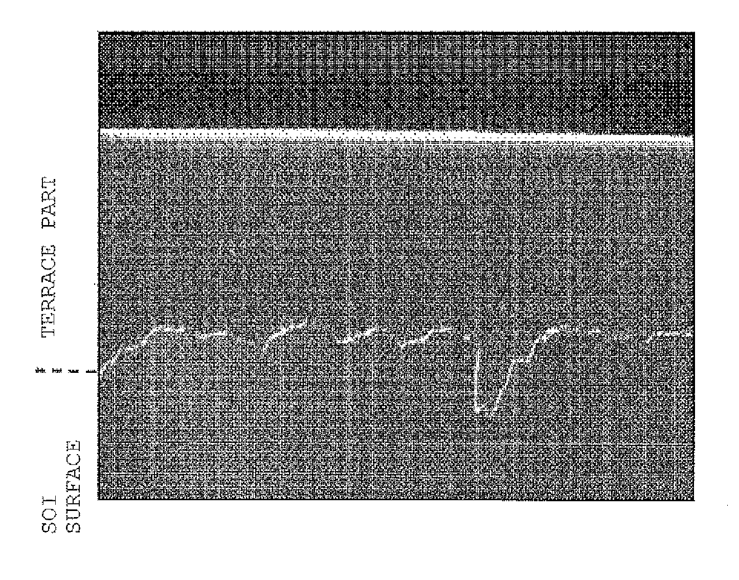
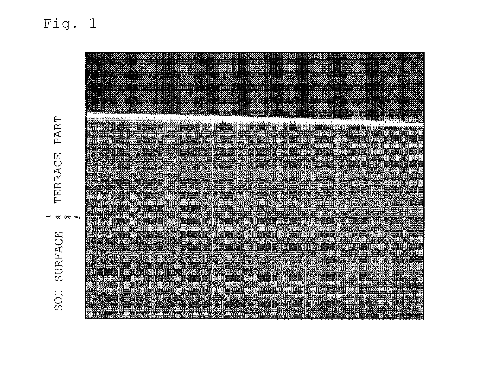
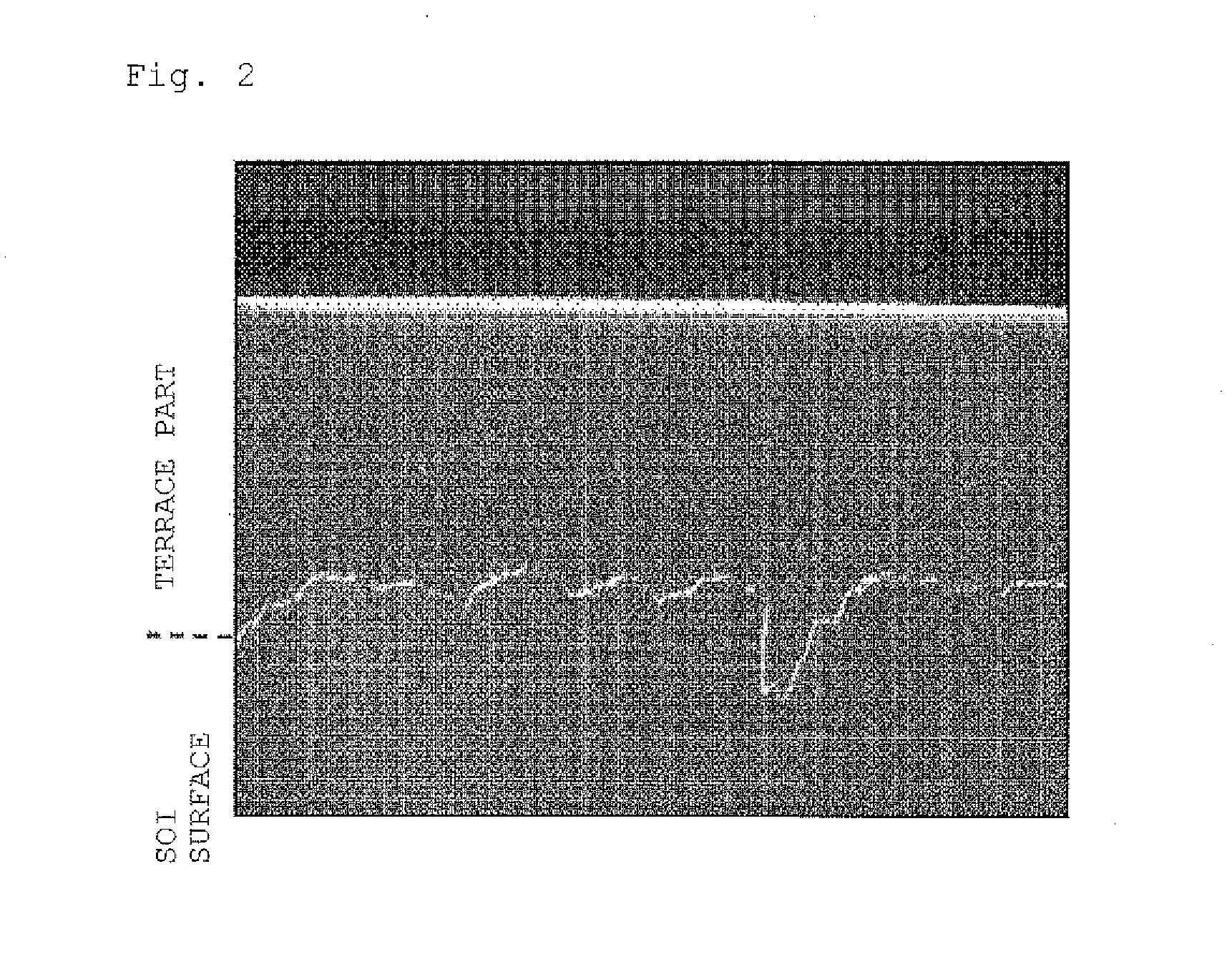
[0069]Finished products of the SOI wafer were produced under the same conditions as in Experimental Example 1 excepting that the heat treatment time in the first step was set to 4 hours, and the second step was set to 3 conditions of 350° C. and 4 hours, 400° C. and 0.5 hours, 450° C. and 0.5 hours were set, and the surface roughness (RMS) of the SOI layer surfaces thereof was measured and compared through the AFM within the range of 30 μm×30 μm. A result is shown in the following Table 3.
TABLE 3RMS (nm)Second350° C.400° C.450° C.First4 h0.5 h0.5 h150° C.4 hNot0.160.17delaminated200° C.4 hNot0.180.17delaminated250° C.4 hNot0.170.19delaminated300° C.4 hNot0.240.25delaminated350° C.4 hNot0.310.30delaminated
[0070]The surface roughness (RMS) of the SOI layer surface when heat treatment was performed for 4 hours within a range of 150° C. to 250° C. as the first step, and heat treatment was performed for 30 minutes at 400° C. to 450° C. as the second step is extremely small. Incidentally,...
PUM
 Abstract
Description
Claims
Application Information
 - R&D Engineer
- R&D Manager
- IP Professional
- Industry Leading Data Capabilities
- Powerful AI technology
- Patent DNA Extraction
Browse by: Latest US Patents, China's latest patents, Technical Efficacy Thesaurus, Application Domain, Technology Topic.
© 2024 PatSnap. All rights reserved.Legal|Privacy policy|Modern Slavery Act Transparency Statement|Sitemap