3D independent double gate flash memory

Active Publication Date: 2015-11-26
MACRONIX INT CO LTD
View PDF7 Cites 145 Cited by
  • Summary
  • Abstract
  • Description
  • Claims
  • Application Information

AI Technical Summary

Benefits of technology

[0011]A 3D memory device configurable for independent double gate, multiple-bit

Problems solved by technology

However, as the channel diameter shrinks, approaching for example 40 nm or less, the field enhancement factor by which the electric field between the word line 15 and the pillar 10 is intensified at the channel surface, can lead to problems with disturbance of charge trapped in the memory cells during read operations and program operations.
As a result, the reliability of the structure degrades.
These multiple-bit-per-cell programmin

Method used


Image

  • 3D independent double gate flash memory
  • 3D independent double gate flash memory
  • 3D independent double gate flash memory

Examples


Embodiment Construction

[0036]A detailed description of embodiments of the present invention is provided with reference to the FIGS. 2-22.

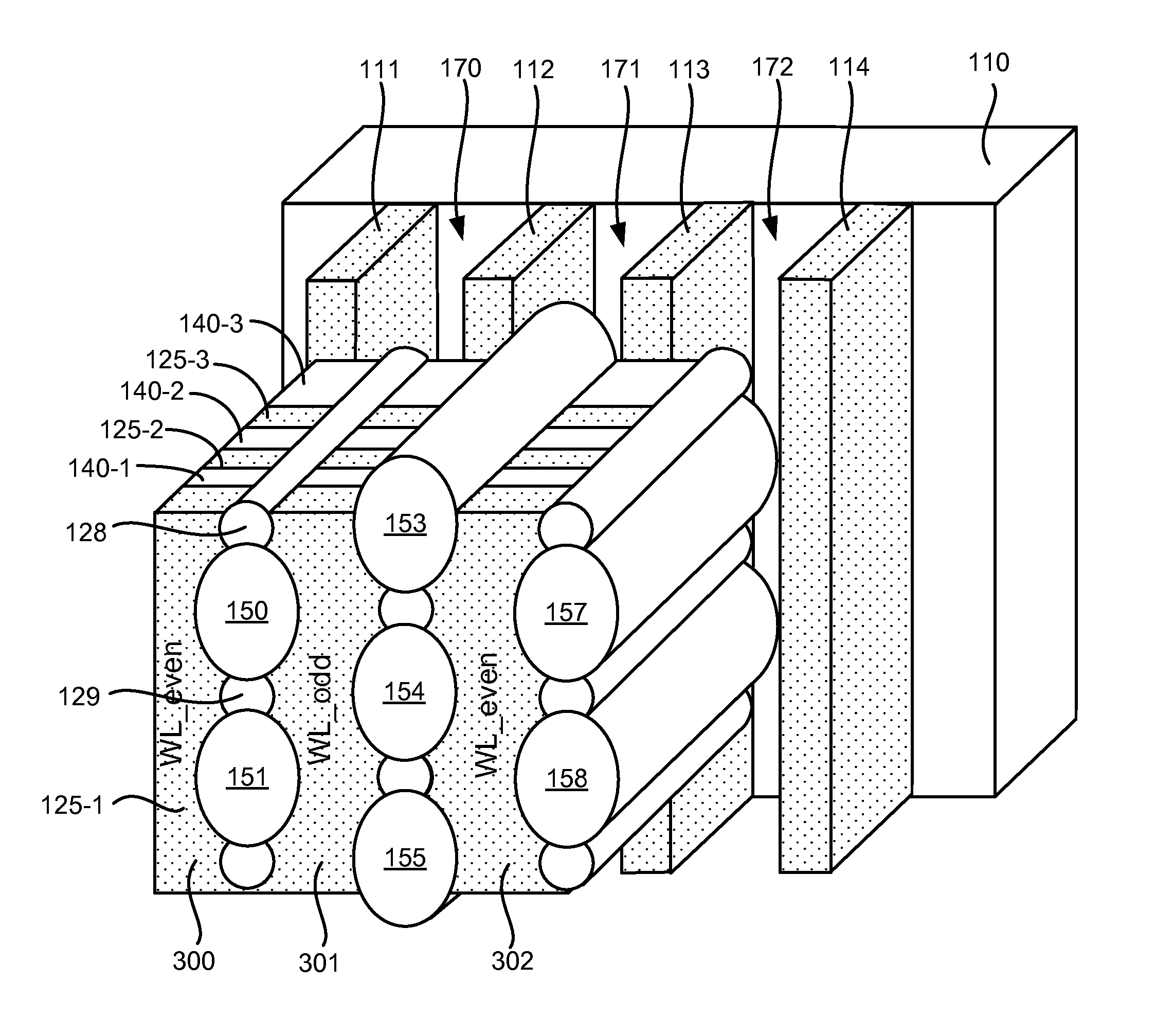
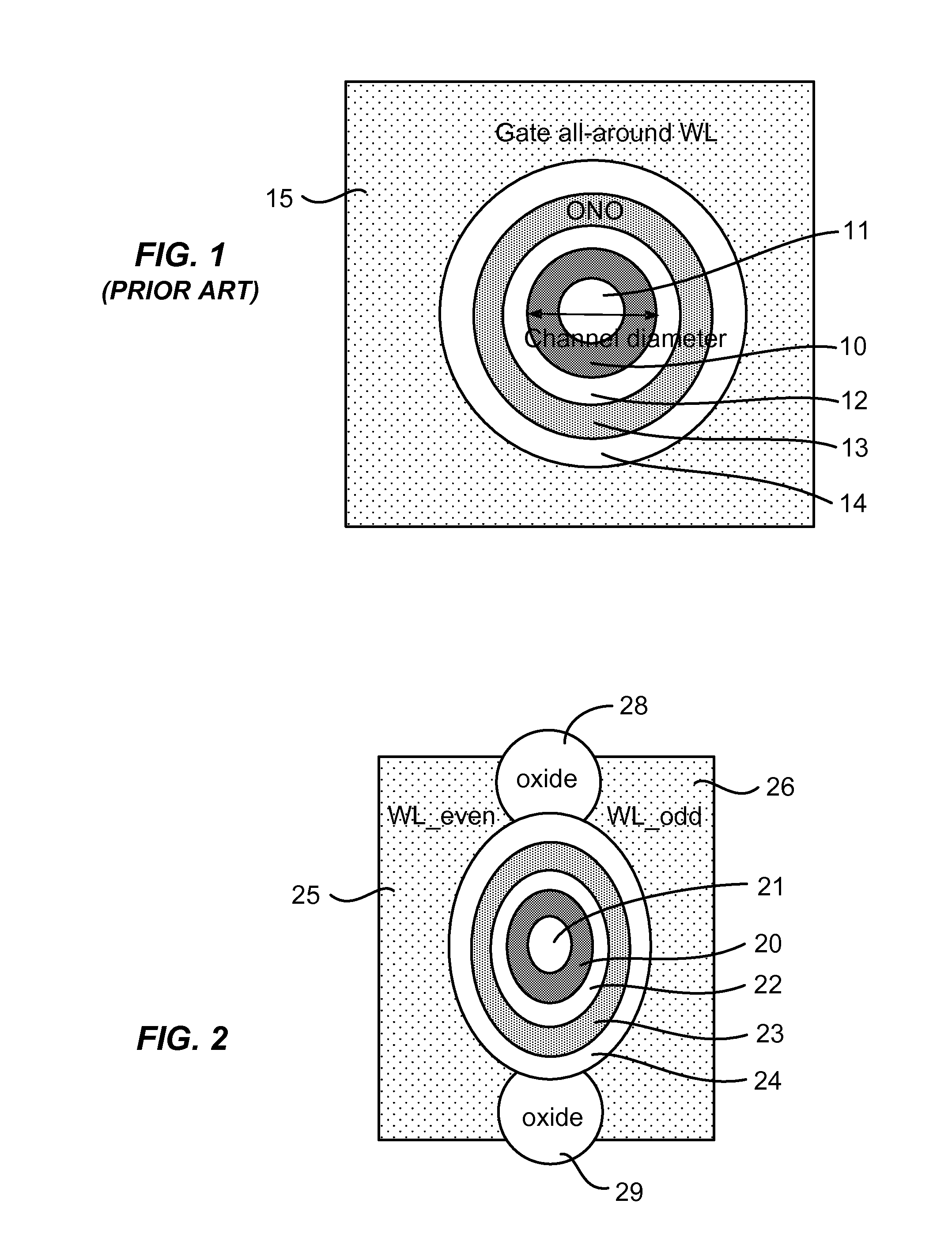
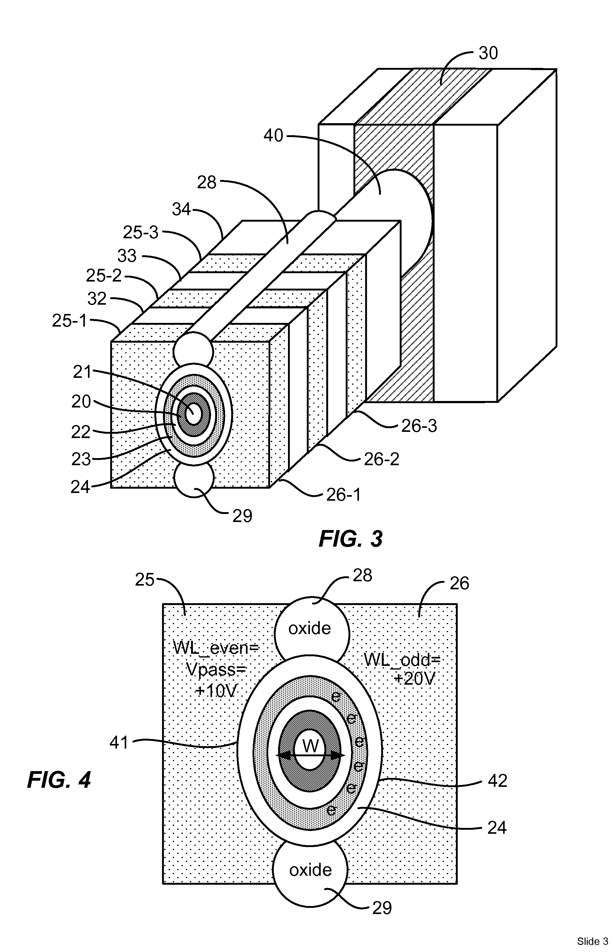
[0037]FIG. 2 is a horizontal cross-section taken through a column of flash memory cells in a 3D array at a word line level. As illustrated, a vertical channel structure 10 of semiconductor material extends vertically through a stack of word line layers. The vertical channel structure 10 may have a seam 21 through the middle. A multilayer dielectric charge trapping structure comprising for example a first layer 22 of silicon oxide, the layer 13 as silicon nitride, and a second layer 24 of silicon oxide, surrounds the vertical channel structure 10. The columnar structure including the vertical channel structure 10 of semiconductor material, and the multilayer dielectric charge trapping structure surrounding the vertical channel structure 10, can be referred to as an active pillar herein.

[0038]An even word line 25 and an odd word line 26 are disposed on opposing sides of th...


PUM


Abstract

A memory device configurable for independent double gate cells, storing multiple bits per cell includes multilayer stacks of conductive strips configured as word lines. Active pillars are disposed between pairs of first and second stacks, each active pillar comprising a vertical channel structure, a charge storage layer and an insulating layer. The insulating layer in a frustum of an active pillar contacts a first arcuate edge of a first conductive strip in a layer of the first stack and a second arcuate edge of a second conductive strip in a same layer of the second stack. A plurality of insulating columns serve, with the active pillars, to divide the stacks of word lines into even and odd lines contacting opposing even and odd sides of each active pillar. The active pillar can be generally elliptical with a major axis parallel with the first and second conductive strips.

Description

BACKGROUND OF THE INVENTION[0001]1. Field of the Invention[0002]The present invention relates to high density memory devices, and particularly to memory devices in which multiple planes of memory cells are arranged to provide a three-dimensional 3D array.[0003]2. Description of Related Art[0004]As critical dimensions of devices in integrated circuits shrink to the limits of common memory cell technologies, designers have been looking to techniques for stacking multiple planes of memory cells to achieve greater storage capacity, and to achieve lower costs per bit. For example, thin film transistor techniques are applied to charge trapping memory technologies in Lai, et al., “A Multi-Layer Stackable Thin-Film Transistor (TFT) NAND-Type Flash Memory,” IEEE Int'l Electron Devices Meeting, 11-13 Dec. 2006; and in Jung et al., “Three Dimensionally Stacked NAND Flash Memory Technology Using Stacking Single Crystal Si Layers on ILD and TANOS Structure for Beyond 30 nm Node,” IEEE Int'l Elec...

Claims


Application Information

Patent Timeline
IPC IPC(8): H01L27/115G11C16/04H01L29/66G11C16/10
CPCH01L27/1157H01L27/11578H01L29/66666G11C16/0466H01L29/66833G11C16/10H01L27/0207G11C11/5671G11C16/0483H01L29/42392H01L29/40117H10B43/27H10B43/35H10B43/00H10B43/20H01L29/792H01L29/7926
Inventor LUE, HANG-TING
Owner MACRONIX INT CO LTD
Why Eureka
Try Eureka