High-voltage Nitride Device and Manufacturing Method Thereof

a high-voltage nitride and manufacturing method technology, applied in the field of microelectronics technology, can solve the problems of high-voltage nitride devices grown on silicon substrates, often caused breakdown of high-voltage nitride devices, and the epitaxial layer vertical breakdown of nitride, etc., to achieve high critical electric field strength, high breakdown voltage, and the effect of increasing the breakdown voltage of high-voltage nitrid

Active Publication Date: 2015-11-26
ENKRIS SEMICON
View PDF1 Cites 5 Cited by
  • Summary
  • Abstract
  • Description
  • Claims
  • Application Information

AI Technical Summary

Benefits of technology

[0024]By removing a part of silicon substrate below the nitride epitaxial layer and between the source electrode and the drain electrode, one or more spatial isolation areas are formed. The nitride epitaxial layer, which can withstand a high voltage, can be isolated from the part of silicon substrate due to the spatial isolation areas, so that a vertical breakdown caused by the silicon substrate can be avoided and a high-voltage nitride device with a high breakdown voltage can be achieved.
[0025]By filling the spatial isolation areas with filling material of high critical electric field strength, and by oxidizing the inner sidewalls of the spatial isolation areas, the breakdown voltage of the high-voltage nitride device can be further increased.
[0026]In order to form at least one spatial area, at least one etched hole is formed in the nitride epitaxial layer; an etching process is implemented in the at least one etched hole to remove off the nitride epitaxial layer and a part of the silicon substrate, and then a selective corrosion process and / or a dry etching process is implemented. The whole process is easy to control, and the production efficiency is greatly improved.

Problems solved by technology

Especially, high-voltage nitride devices are drawing extensive attention of researchers all over the world because of their superior performance and great potential.
When applying a high voltage to a high-voltage nitride device grown on a silicon substrate, the silicon substrate considered as a low resistance area is a path of the leakage current, since the critical electric field of silicon is low and the silicon material itself is electric conductive; and when the applied voltage is too high and the applied electric field exceeds the critical value, a breakdown may occur in the silicon substrate, which may further lead to a vertical breakdown of the nitride epitaxial layer.
Generally speaking, the breakdown of the high-voltage nitride device grown on a silicon substrate is often caused by the vertical breakdown.
Due to the lattice and thermal mismatch between silicon and nitride layers, the thickness of the nitride epitaxial layer is greatly limited (about 2 μm˜4 μm generally).
In addition, a thicker epitaxial layer requires more material and more growth time, which greatly increases cost and decreases production capacity.
Furthermore, the increasing of the thickness of the nitride epitaxial layer may lead to more defects including dislocations in the nitride epitaxial layer.
However, the silicon substrate used for nitride layer growth is usually very thick (several hundred μm or even greater than 1 mm), and thus the etching process is complex and difficult.

Method used


Image

  • High-voltage Nitride Device and Manufacturing Method Thereof
  • High-voltage Nitride Device and Manufacturing Method Thereof
  • High-voltage Nitride Device and Manufacturing Method Thereof

Examples


Embodiment Construction

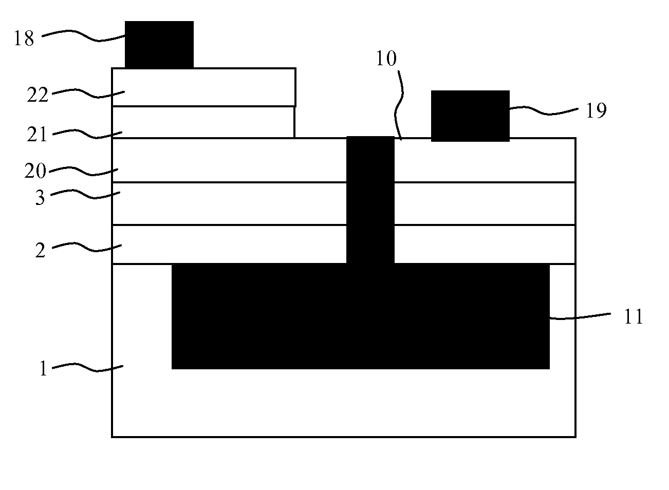
[0046]In an embodiment of the present invention, a high-voltage nitride device includes:

[0047]a silicon substrate;

[0048]a nitride epitaxial layer, prepared on the silicon substrate;

[0049]a source electrode and a drain electrode, both of which are contacted with the nitride epitaxial layer;

[0050]a gate electrode, prepared between the source electrode and the drain electrode; and,

[0051]at least one spatial isolation area, formed in a region between the silicon substrate and the nitride epitaxial layer vertically and between the source electrode and the drain electrode horizontally.

[0052]In an embodiment of the present invention, the nitride epitaxial layer consists of a nitride nucleation layer, a nitride buffer layer and a nitride channel layer. Furthermore, since the area between the gate electrode and the drain electrode is the main voltage withstanding area, the at least one spatial isolation area is formed between the gate electrode and the drain electrode horizontally. In this c...


PUM

PropertyMeasurementUnit
thicknessaaaaaaaaaa
breakdown voltageaaaaaaaaaa
thickaaaaaaaaaa

Abstract

A high-voltage nitride device which can avoid vertical breakdown and has a high breakdown voltage includes: a silicon substrate; a nitride epitaxial layer, prepared on the silicon substrate; a source electrode and a drain electrode, both of which are contacted with the nitride epitaxial layer; a gate electrode, prepared between the source electrode and the drain electrode; and, at least one spatial isolation area, formed in a region between the silicon substrate and the nitride epitaxial layer vertically and between the source electrode and the drain electrode horizontally.

Description

CROSS-REFERENCE TO RELATED APPLICATION[0001]This application is Continuation-In-Part application of PCT application Serial No. PCT / CN2014 / 070148, filed on Jan. 6, 2014 which claims priority from Chinese Patent Application Serial No. 201310049853.X, filed on Feb. 7, 2013, the entire contents of which are incorporated herein by reference for all purposes.FIELD OF THE INVENTION[0002]The present invention is related to micro-electronics technology, and more particularly to a high-voltage nitride device and a manufacturing method thereof.BACKGROUND OF THE INVENTION[0003]Because of having a wide band gap, high electron saturation drift velocity, high critical electric field and high thermal conductivity, wide band gap compounds show great potential in application fields of high frequency, high temperature and high power. Especially, high-voltage nitride devices are drawing extensive attention of researchers all over the world because of their superior performance and great potential.[0004...

Claims


Application Information

Patent Timeline
Patent Type & Authority Applications(United States)
IPC IPC(8): H01L29/778H01L29/205H01L21/3065H01L29/06H01L21/02H01L21/306H01L29/20H01L29/66
CPCH01L29/7787H01L29/2003H01L29/205H01L29/66462H01L21/3065H01L21/02381H01L21/0254H01L21/02458H01L21/30612H01L29/0649H01L29/1083H01L29/66522H01L29/78
Inventor CHENG, KAI
Owner ENKRIS SEMICON
Why Eureka
Try Eureka