
Gas barrier film, film substrate provided with gas barrier film, and electronic device including the film substrate

a technology of gas barrier film and film substrate, which is applied in the direction of superimposed coating process, application, instruments, etc., can solve the problems of deterioration of display elements (e.g., organic el elements) formed on the film substrate, inferior gas barrier properties of glass substrates, etc., and achieve high gas barrier properties and high bending resistance

Active Publication Date: 2015-12-03
SAMSUNG DISPLAY CO LTD
View PDF3 Cites 314 Cited by
  • Summary
  • Abstract
  • Description
  • Claims
  • Application Information

AI Technical Summary

Benefits of technology

The patent describes a gas barrier film made of inorganic layers that can be used to create electronic devices with high gas barrier properties and bending resistance. The gas barrier film has alternating layers made of different inorganic materials, with each layer having a specific thickness. This structure allows for a high gas barrier property and also allows for bending without compromising the gas barrier property. The details of the technique and its effects can be found in the patent text.

Problems solved by technology

Film substrates are, however, inferior to glass substrates in the gas barrier property.
Display elements (e.g., organic EL elements) formed on a film substrate has a risk of being deteriorated with time by being brought into contact with water and oxygen infiltrated through the film substrate during the use of the display.

Method used


Image

  • Gas barrier film, film substrate provided with gas barrier film, and electronic device including the film substrate
  • Gas barrier film, film substrate provided with gas barrier film, and electronic device including the film substrate
  • Gas barrier film, film substrate provided with gas barrier film, and electronic device including the film substrate

Examples


embodiments

Structure of Gas Barrier Film

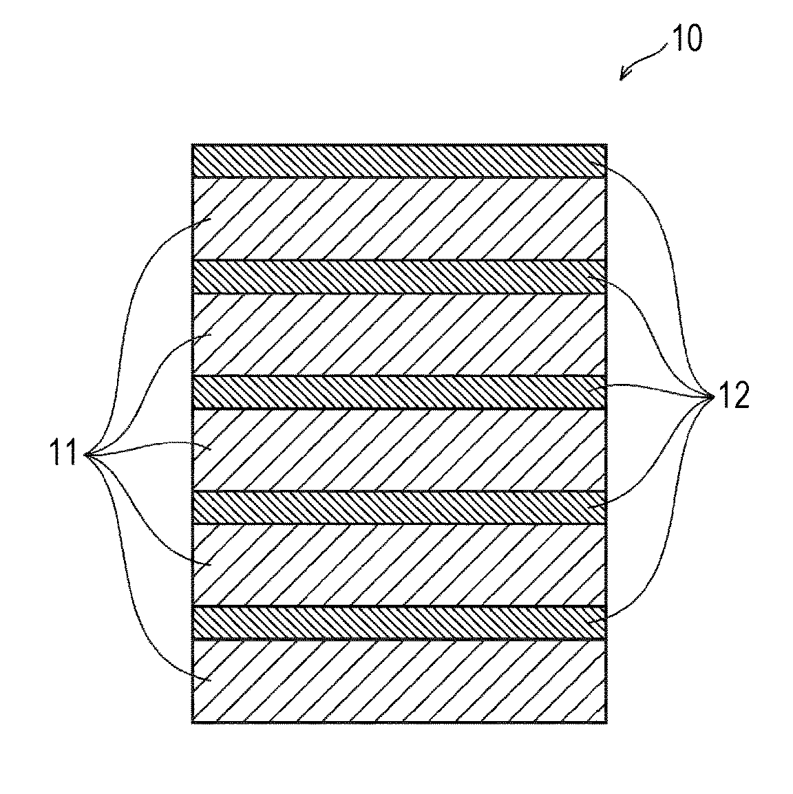
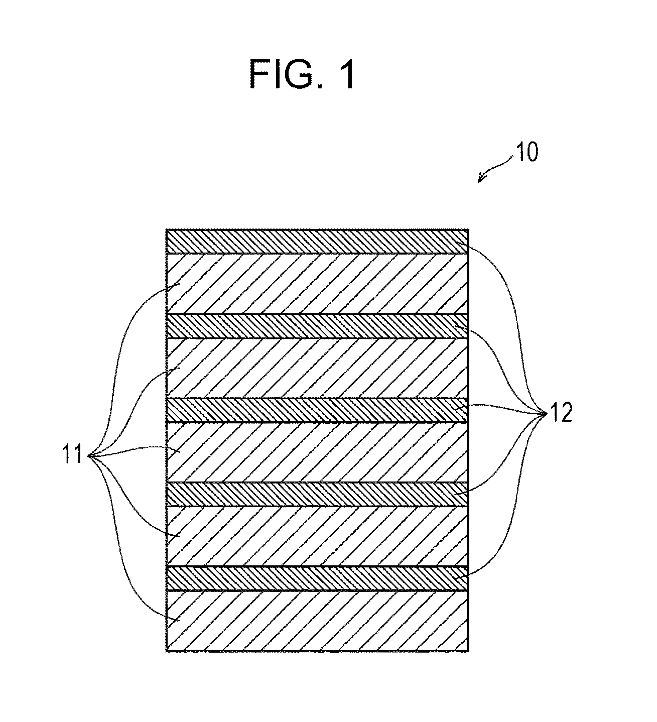
[0044]FIG. 1 is a cross-sectional view schematically illustrating a gas barrier film according to an embodiment of the present disclosure. The gas barrier film 10 has a multilayer structure including first barrier layers 11 and second barrier layers 12 that are alternately stacked. The multilayer structure shown in FIG. 1 is composed of five first barrier layers 11 and five second barrier layers 12. Structure of first and second barrier layers

[0045]The first barrier layers 11 are made of a first inorganic material. The first inorganic material can be aluminum oxide. An aluminum oxide film has a high gas barrier property.

[0046]The second barrier layers 12 are made of a second inorganic material. The second inorganic material can be, for example, an oxide of at least one metal selected from the group consisting of zirconium, zinc, silicon, titanium, hafnium, tantalum, and lanthanum. The second inorganic material can be, for example, a nitride or an oxynitr...

experiment 1

[0060]Gas barrier film samples having different structures formed under different conditions were prepared. The water vapor transmission rates of the individual samples were compared. The structures and film-forming conditions of the samples were as follows.

Sample 1

[0061]FIG. 5A is a schematic cross-sectional view of the gas barrier film sample 1

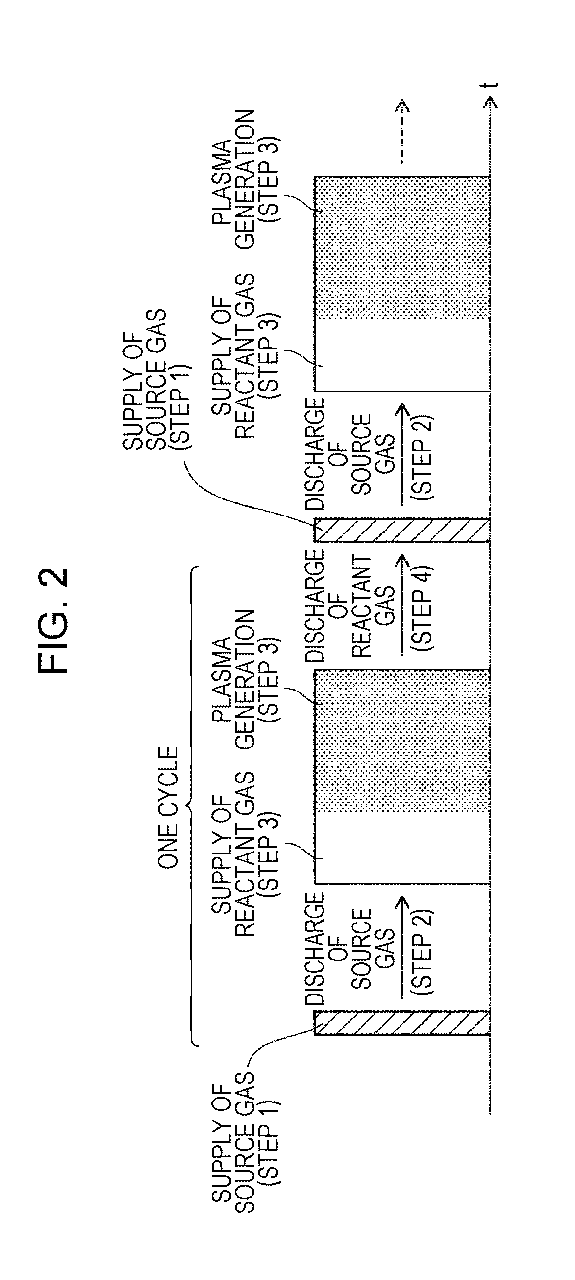
[0062]An aluminum oxide film 11A was formed on a polyimide film having a thickness of 38 μm by plasma ALD using trimethyl aluminum (TMA: Al(CH3)3) as a source gas, Ar as a purge gas, and O2 as a reactant gas. A gas barrier film having a thickness of 20 nm was formed through 200 cycles of atomic film formation at a TMA supply time of 0.06 sec, an O2 supply time of 20 sec, a plasma exposure time of 17 sec, a TMA discharge time of 5 sec, and an O2 discharge time of 5 sec. The time for one cycle was about 30 sec, and the total time for the 200 cycles was about 100 min.

Sample 2

[0063]FIG. 5B is a schematic cross-sectional view of the gas barrier f...

experiment 2

[0074]As shown in FIGS. 8A to 8F, gas barrier film samples each having a thickness of 20 nm and one, two, three, four, five, or ten AlO / ZrO lamination units were prepared. In the one-tier structure, the aluminum oxide film had a thickness of 19 nm, and the zirconium oxide film had a thickness of 1 nm. In the two-tier structure, each aluminum oxide film had a thickness of 9 nm, and each zirconium oxide film had a thickness of 1 nm. In the three-tier structure, each aluminum oxide film had a thickness of 5.7 nm, and each zirconium oxide film had a thickness of 1 nm. In four-tier structure, each aluminum oxide film had a thickness of 4 nm, and each zirconium oxide film had a thickness of 1 nm. In five-tier structure, each aluminum oxide film had a thickness of 3 nm, and each zirconium oxide film had a thickness of 1 nm. In ten-tier structure, each aluminum oxide film had a thickness of 1 nm, and each zirconium oxide film had a thickness of 1 nm. Table 1 shows the structures of the samp...


PUM

PropertyMeasurementUnit
Thicknessaaaaaaaaaa
Thicknessaaaaaaaaaa
Nanoscale particle sizeaaaaaaaaaa

Abstract

A gas barrier film includes two or more first barrier layers each made of a first inorganic material and one or more second barrier layers each made of a second inorganic material different from the first inorganic material. Each of the two or more first barrier layers and each of the one or more second barrier layers are alternately stacked. The first inorganic material comprises aluminum oxide. Each of the two or more first barrier layers has a thickness of 3 nm or more. The total thickness of the two or more first barrier layers is 20 nm or less. The two or more first barrier layers and the one or more second barrier layers are formed by atomic layer deposition.

Description

BACKGROUND[0001]1. Technical Field[0002]The present disclosure relates to a gas barrier film made of an inorganic material, a film substrate provided with the gas barrier film, and an electronic device including the film substrate.[0003]2. Description of the Related Art[0004]Displays mounted on, for example, portable information terminals are required to be reduced in thickness and weight. Recently, demands for displays having high shock resistance and high flexibility, in addition to the reduced thickness and weight, are growing. Accordingly, film substrates made of resin materials have been investigated as substrates for displays, instead of the existent glass substrates.[0005]Film substrates are, however, inferior to glass substrates in the gas barrier property. Display elements (e.g., organic EL elements) formed on a film substrate has a risk of being deteriorated with time by being brought into contact with water and oxygen infiltrated through the film substrate during the use ...

Claims


Application Information

Patent Timeline
IPC IPC(8): B32B9/04
CPCB32B9/04Y10T428/265B32B2457/00B32B2307/7242C23C28/042C23C16/403C23C16/405C23C28/42H10K59/8731H10K50/8445
Inventor SHIBATA, MASAOMIOKUMOTO, KENJISAKAMOTO, GOSUKE
Owner SAMSUNG DISPLAY CO LTD
Learn More