Semiconductor Device and Electronic Device

a technology of semiconductor devices and electronic devices, applied in emergency protective circuit arrangements, transistors, etc., can solve the problems of unstable operation of semiconductor devices, low surge immunity, and the protection circuit itself may break, so as to reduce the area of protection circuits and reduce the surge immunity

Inactive Publication Date: 2015-12-03
SEMICON ENERGY LAB CO LTD
View PDF2 Cites 31 Cited by
  • Summary
  • Abstract
  • Description
  • Claims
  • Application Information

AI Technical Summary

Benefits of technology

[0014]With the progress of miniaturization and integration of a semiconductor device, it is desired to reduce the area of a protection circuit. However, miniaturization of an element used in the protection circuit may lower the surge immunity and thereby the protection circuit itself may break in some cases.

Problems solved by technology

However, miniaturization of an element used in the protection circuit may lower the surge immunity and thereby the protection circuit itself may break in some cases.
Therefore, in the case where a protection circuit including such an element is connected between a wiring (e.g., a signal line) connected to a semiconductor circuit and a power supply line, a leak current may flow between the wirings to change the potentials of the wirings or the power supply potential, causing unstable operation of the semiconductor device.

Method used


Image

  • Semiconductor Device and Electronic Device
  • Semiconductor Device and Electronic Device
  • Semiconductor Device and Electronic Device

Examples


embodiment 1

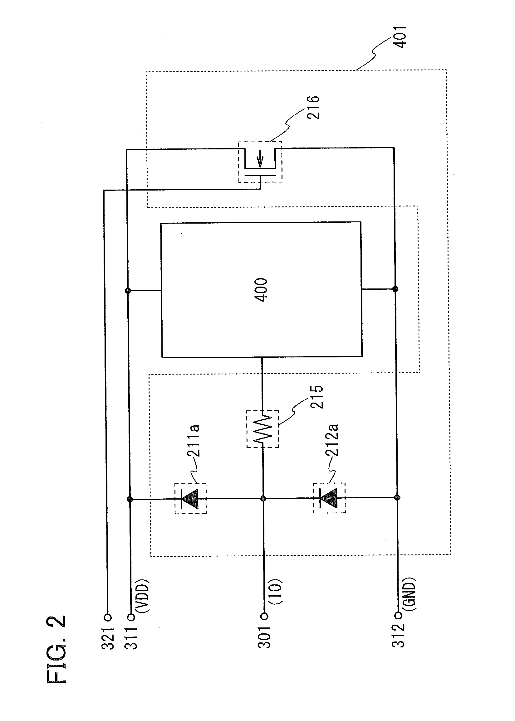
[0070]In this embodiment, a semiconductor element which can be used in a protection circuit of one embodiment of the present invention.

[Semiconductor Element]

[0071]To prevent a large amount of current due to ESD from flowing in an integrated circuit, a protection circuit is preferably provided between an input portion of the integrated circuit (i.e., an external terminal) and the integrated circuit, and a path for discharging a large current is preferably provided in the protection circuit. In some cases, a large current flows in a short time due to ESD. In that case, for example, when the discharge path has high resistance, current flows in another path such as an integrated circuit portion, which might result in breakdown of elements in a circuit. Thus, the path for discharging current due to ESD preferably has lower resistance than that of a path connected from an external terminal to an inside of the integrated circuit.

[0072]Here, the external terminal is an input portion to a w...

embodiment 2

[0154]In this embodiment, an example of a transistor which can be used for the circuits shown in Embodiment 1 is described.

[Structure of Transistor]

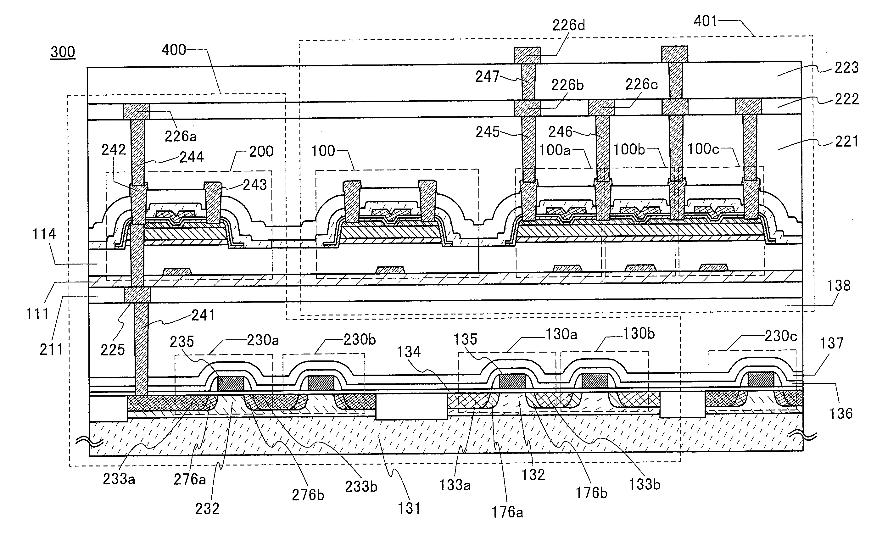
[0155]FIGS. 16A to 16E illustrate an example of a field effect transistor using one embodiment of the present invention. FIG. 16A is a top view of the transistor 100. FIG. 16B shows a cross section taken along dashed dotted line X-X′ in FIG. 16A, and FIG. 16D is a cross section taken along dashed dotted line Y-Y′ in FIG. 16D. The transistor 100 in FIGS. 16A to 16E includes a substrate 50, an insulating film 51 in contact with a top surface of the substrate 50, an insulating film 114 in contact with a top surface of the insulating film 51, a semiconductor layer 101 in contact with a top surface of the insulating film 114, conductive layers 104a and 104b, a gate insulating film 102 over the semiconductor layer 101, and a gate electrode 103 overlapping the semiconductor layer 101 with the gate insulating film 102 positioned therebetween. Th...

embodiment 3

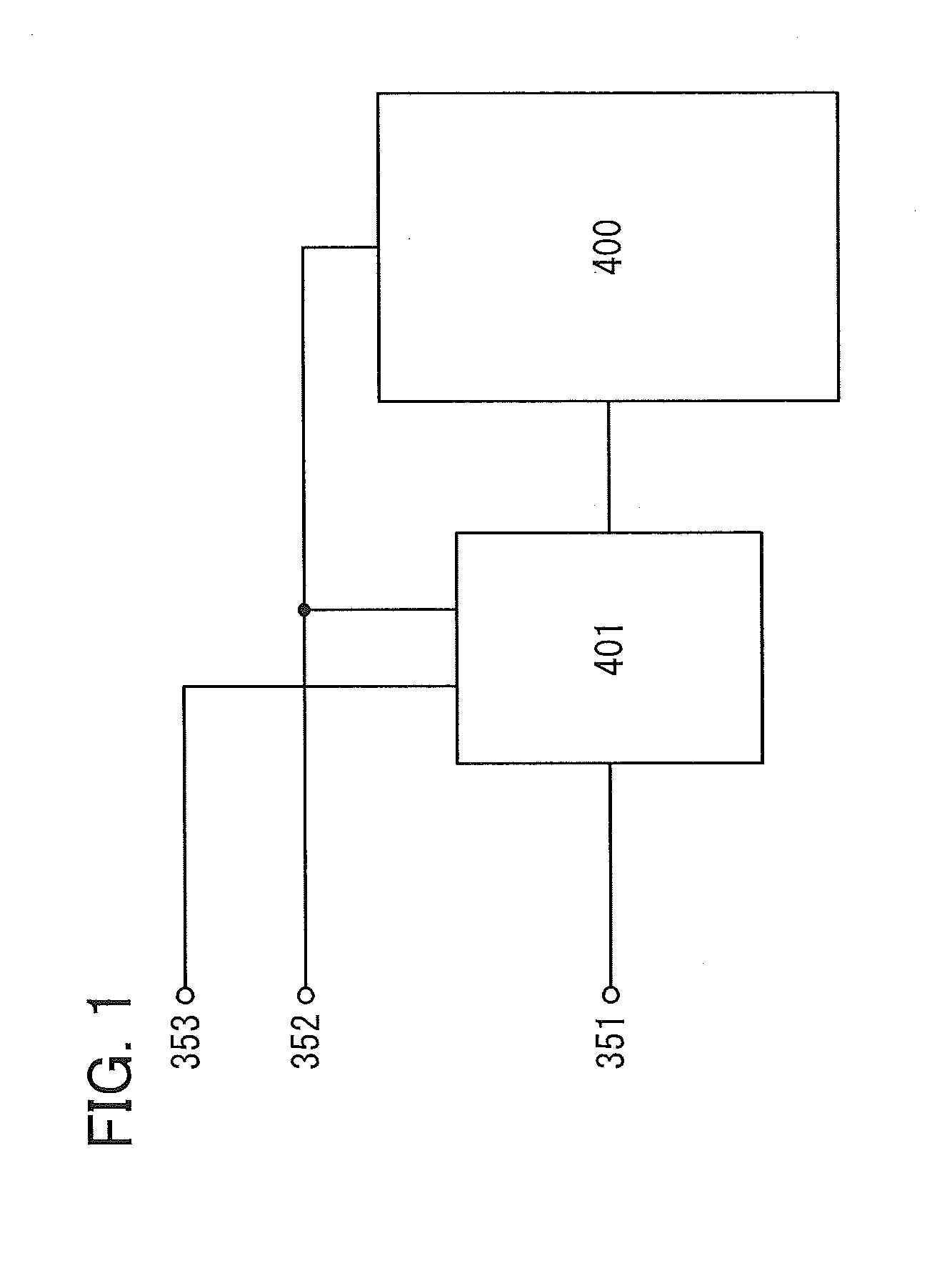
[0225]In this embodiment, an example of a semiconductor device including the protection circuit and the integrated circuit in one embodiment of the present invention is described.

[Integrated Circuit 400]

[0226]FIG. 22 illustrates an example of a semiconductor device 300. The semiconductor device 300 includes the integrated circuit 400 and the protection circuit 401. The integrated circuit 400 includes a semiconductor element. Examples of the semiconductor element are preferably a semiconductor material such as silicon, germanium, gallium, and arsenic; compound semiconductor material containing silicon, germanium, gallium, arsenic, or aluminum; organic semiconductor material; and oxide semiconductor materials.

[0227]The integrated circuit 400 preferably includes a transistor. The transistor included in the integrated circuit 400 includes a region where a channel length is preferably less than or equal to 60 nm, more preferably less than or equal to 40 nm, and still more preferably less...


PUM


Abstract

A semiconductor device that is hardly broken is provided. Alternatively, a semiconductor device having high reliability is provided. The semiconductor device includes a first circuit, a second circuit, a first wiring, a second wiring, and a third wiring. The second circuit has a function of protecting the first circuit. The second circuit includes a first transistor including an oxide semiconductor film. The first wiring is electrically connected to the first circuit through the second circuit. The first wiring is electrically connected to the first circuit through the second circuit. The first wiring has a function of inputting a signal. The second wiring is electrically connected to the first circuit. The second wiring is electrically connected to one of a source electrode and a drain electrode of the first transistor. The third wiring is electrically connected to a gate electrode of the first transistor included in the second circuit.

Description

BACKGROUND OF THE INVENTION[0001]1. Field of the Invention[0002]The present invention relates to an object, a method, or a manufacturing method. In addition, the present invention relates to a process, a machine, a manufacture, or a composition of matter. Another embodiment of the present invention relates to a semiconductor device, a display device, a lighting device, a power storage device, a memory device, or a driving method or manufacturing method thereof. Specifically, one embodiment of the present invention relates to a semiconductor device provided with a means of preventing a circuit from being damaged by unexpected high-voltage application such as electrostatic discharge.[0003]In this specification and the like, a semiconductor device generally means a device that can function by utilizing semiconductor characteristics. A transistor and a semiconductor circuit are embodiments of semiconductor devices. An arithmetic device, a memory device, an imaging device, an electro-opt...

Claims


Application Information

Patent Timeline
Patent Type & Authority Applications(United States)
IPC IPC(8): H01L27/02H01L23/528H01L27/12H01L29/786
CPCH01L27/0266H01L29/7869H01L23/528H01L29/78696H01L27/0288H01L27/1207H01L27/0255H01L23/60H01L27/1225H01L2924/0002H01L2924/00
Inventor ISOBE, ATSUO
Owner SEMICON ENERGY LAB CO LTD
Why Eureka
Try Eureka