Operational amplifier

a technology of operation amplifier and amplifier, which is applied in the direction of amplifier with semiconductor device/discharge tube, amplifier using switched capacitor, etc., can solve the problem of absolute loss of circuit gain, and achieve the effect of effective operation and decreasing gain

Inactive Publication Date: 2015-12-10
NAT INST OF ADVANCED IND SCI & TECH
View PDF4 Cites 13 Cited by
  • Summary
  • Abstract
  • Description
  • Claims
  • Application Information

AI Technical Summary

Benefits of technology

[0017]According to the present invention, by providing a high-pass filter on the input side of a differential amplifier that amplifies an input signal pair modulated by a chopper, and setting the bias point of the differential-amplifier input node within a common-mode range in which the differential amplifier is operable, the differential amplifier can be operated effectively regardless of the possible decrease in a supply voltage without decreasing gain, enabling normal amplifying operation.

Problems solved by technology

There is also a problem that, in the conventional operational amplifier described above, when the operational voltage (VDD−VSS) decreases, the circuit gain would absolutely decrease.

Method used


Image

  • Operational amplifier
  • Operational amplifier
  • Operational amplifier

Examples


first embodiment

Second Variation of First Embodiment

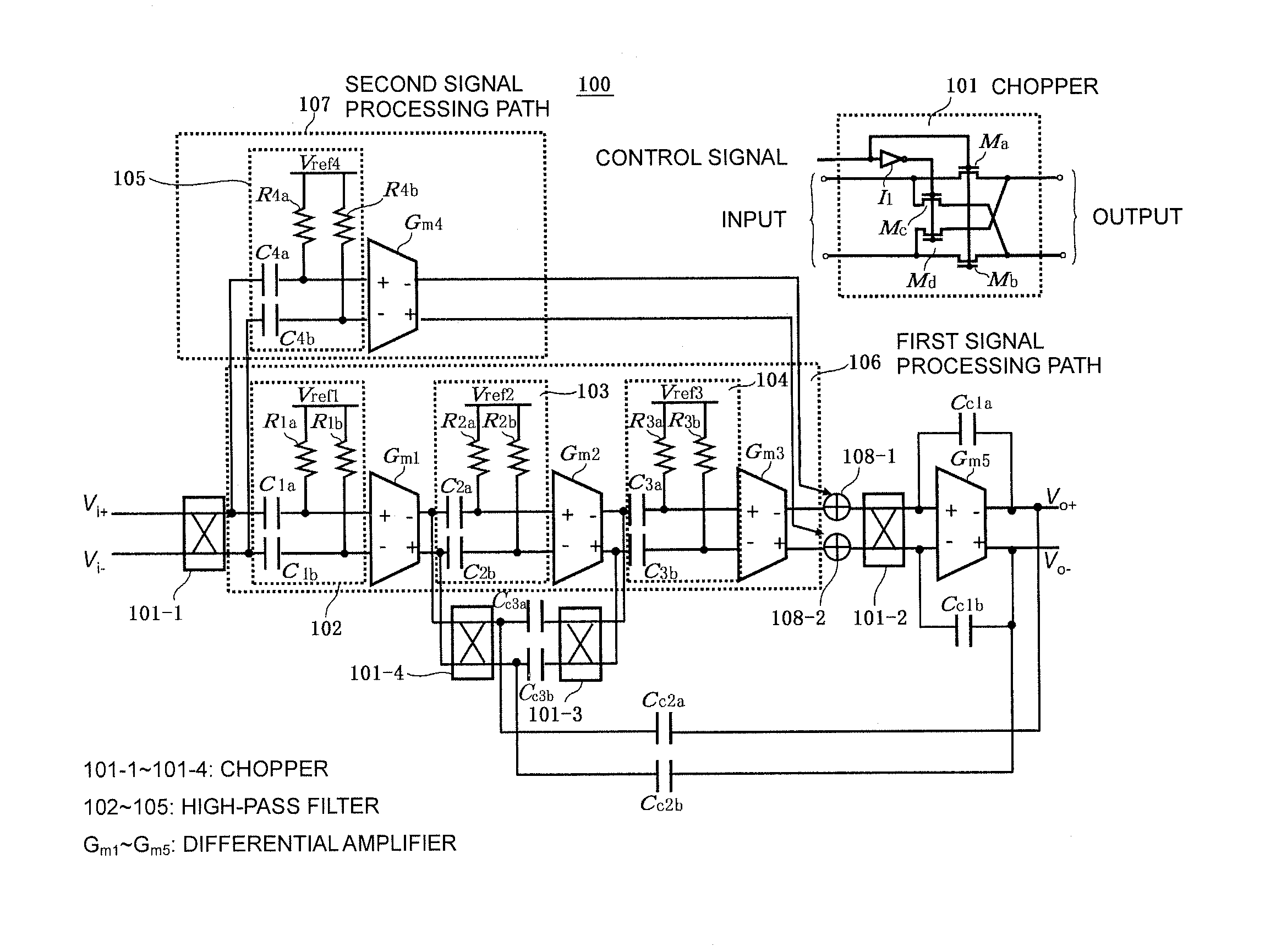
[0050]In the embodiment and its variation shown in FIGS. 1 and 4, the high-pass filter 103 can be omitted accordingly in such a case that the differential amplifier Gm2 receives the outputs from the differential amplifier Gm1 as they are.

second embodiment

[0051]FIG. 5 shows the circuit diagram of a second embodiment of the operational amplifier according to the present invention. In this figure, the same components as those in FIG. 4 are denoted by the same symbols. An operational amplifier 500 of the second embodiment shown in FIG. 5 is a chopper-stabilized operational amplifier operating as a fully differential amplifier by including two circuit units 151a and 151b equivalent to the circuit unit 151 enclosed by the dashed line in FIG. 4 to serve as third and fourth signal processing paths, respectively, providing a class-AB amplifier for non-inverted output 501 and a class-AB amplifier for inverted output 502, inputting inverted signals output from the respective third and fourth signal processing paths 151a, 151b to the class-AB amplifier for non-inverted output 501 through the choppers, and inputting non-inverted signals output from the respective third and fourth signal processing paths 151a, 151b to the class-AB amplifier for i...

third embodiment

[0060]FIG. 6 shows the circuit diagram of a third embodiment of the operational amplifier according to the present invention. In this figure, the same components as those in FIG. 1 are denoted by the same symbols, and the explanation thereof is omitted. An operational amplifier 600 of the third embodiment shown in FIG. 6 is a chopper-stabilized operational amplifier where the circuit unit from the output stage of the differential amplifier Gm1 to the input stage of the summing elements 108-1, 108-2 in the operational amplifier 100 of the first embodiment shown in FIG. 1 is replaced by a high-pass filter 109, a non-inverting differential amplifier Gm20, and a chopper 101-8.

[0061]In other words, in FIG. 6, the output nodes (non-inverting and inverting output terminals) of the differential amplifier Gm1 are connected to the input nodes (non-inverting and inverting input terminals) of the non-inverting differential amplifier Gm20 via the high-pass filter 109. The high-pass filter 109 in...


PUM


Abstract

There is provided an operational amplifier which is operable as well when an operating voltage decreases without creating a range where a circuit would not operate or reducing circuit gain. High-pass filters 102-105 provide output signals therefrom to bias-set input nodes of differential amplifiers Gm1-Gm4 to a potential within a common-mode range in which the respective differential amplifiers Gm1-Gm4 are operable. In this manner, the respective differential amplifiers Gm1-Gm4 can be operated effectively regardless of the possible decrease in a supply voltage, enabling normal amplifying operation. In addition, reduction in gain due to the reduced operational voltage is avoided. Therefore, it is preferably applicable to the application where digital and analog circuits are loaded together on the same IC chip. When a high-pass filter is required at each input side of two- or more-stage differential amplifiers, a phase compensation method utilizing multiple paths is provided for a lower range of a phase margin created at the low frequency side, enabling normal amplitude operation.

Description

BACKGROUND OF THE INVENTION[0001]1. Field of the Invention[0002]The present invention relates to an operational amplifier, and in particular, to a chopper-stabilized operational amplifier in which input signal pairs are modulated by a first chopper to be amplified in a signal processing path configured by one or more differential amplifier stages, and the amplified modulated signals are demodulated by a second chopper for output.[0003]2. Description of the Related Art[0004]There is an advantage in creating an analog circuit and a digital circuit on the same integrated circuit (IC) chip in terms of reduction in the cost of a system. However, implementing the digital and analog circuits together on the same IC chip adds the constraints imparted to the analog circuit design. One of such constraints is decrease in an operating voltage range resulting from supply voltage scaling. In other words, when supply voltage scaling is necessary to scale down the device size in digital circuits, a...

Claims


Application Information

Patent Timeline
Patent Type & Authority Applications(United States)
IPC IPC(8): H03F3/393H03F3/45
CPCH03F3/393H03F3/45179H03F2200/271H03F2200/405H03F2203/45544H03F3/005H03F3/45192H03F3/45475H03F2200/168H03F2200/249H03F2203/45366H03F2203/45512H03F2203/7212
Inventor OUCHI, SHINICHI
Owner NAT INST OF ADVANCED IND SCI & TECH
Why Eureka
Try Eureka