Package structure and method of manufacturing the same

a packaging structure and manufacturing method technology, applied in the direction of printed element electric connection formation, non-printed electrical components of printed circuits, semiconductor/solid-state device details, etc., can solve the problems of poor quality, low yield rate of packaging structure b>1/b>, blind hole and via thus formed, etc., to increase electrical performance and signal stability, reduce the overall size of the package structure, and reduce the effect of siz

Active Publication Date: 2015-12-10
PHOENIX PIONEER TECH
View PDF5 Cites 14 Cited by
  • Summary
  • Abstract
  • Description
  • Claims
  • Application Information

AI Technical Summary

Benefits of technology

The patent describes a package structure and manufacturing method that includes two layers of wirings and an opening on a second insulating layer. This design utilizes unoccupied regions and reduces the overall size of the package structure. Additionally, the second wiring layer improves electrical performance and signal stability. The invention does not require a core board and has a smaller size and higher layout usage rate. It also ensures secure positioning of electronic components without displacement.

Problems solved by technology

Therefore, the package structure 1 has a low yield rate and poor quality.
The blind holes and vias thus formed can be circular only, and have poor quality.
The attachment and detachment of the PI tapes to and from the carrier board 10 adversely increase the overall cost of the package structure 1.
The additional lamination and cure process increase the overall cost and time required to manufacture the package structure 1, and may lead to displacement of the semiconductor chip 18 (or even rotation).
As a result, the electrical connection is poor, and the package structure 1 thus has a low yield rate.
In the conventional package structure 1′, since the copper coil substrate is used as the carrier board 10, it is easy to cause delamination, and the package structure 1′ is damaged.
However, the laser process can form circular blind holes only, and the blind holes have poor quality.
Furthermore, since attaching the passive component 18′ is achieved through non-conductive material and a dispensing method, the diameter of dispensing adhesive is larger than 200 μm and is difficult to control the volume of each dispensing adhesive, it is very easy for the insulating adhesive material 180′ to spread to other areas, causing the wirings between each of the first wiring layer 11′ to attach to the adhesive, thereby undesirably lowering the reliability.
After another two processes of making the dielectric material layer, the dielectric encapsulating layer 16′ is formed by a lamination process, however as the first dielectric material layer 13 and the second dielectric material layer can be mistakenly placed, not only this increases the time and cost, because the passive component 18′ has not yet been secured in place before baking the passive component 18′, but also the passive component 18′ may easily become displaced, causing a loss in yield.
In addition, using conductors 15 as a means to electrically connect the passive component 18′ may increase the electrical pathway and signal loss, and the cost of using copper electrodes (MLCC) as the passive component 18′ is also very high.

Method used


Image

  • Package structure and method of manufacturing the same
  • Package structure and method of manufacturing the same
  • Package structure and method of manufacturing the same

Examples


Embodiment Construction

[0032]The present invention is described in the following with specific embodiments, so that one skilled in the pertinent art can easily understand other advantages and effects of the present invention from the disclosure of the present invention.

[0033]It should be noted that all the drawings are not intended to limit the present invention. Various modification and variations can be made without departing from the spirit of the present invention. Further, terms, such as “upper”, “lower”, “first”, “second” and “one” etc., are merely for illustrative purpose and should not be construed to limit the scope of the present invention.

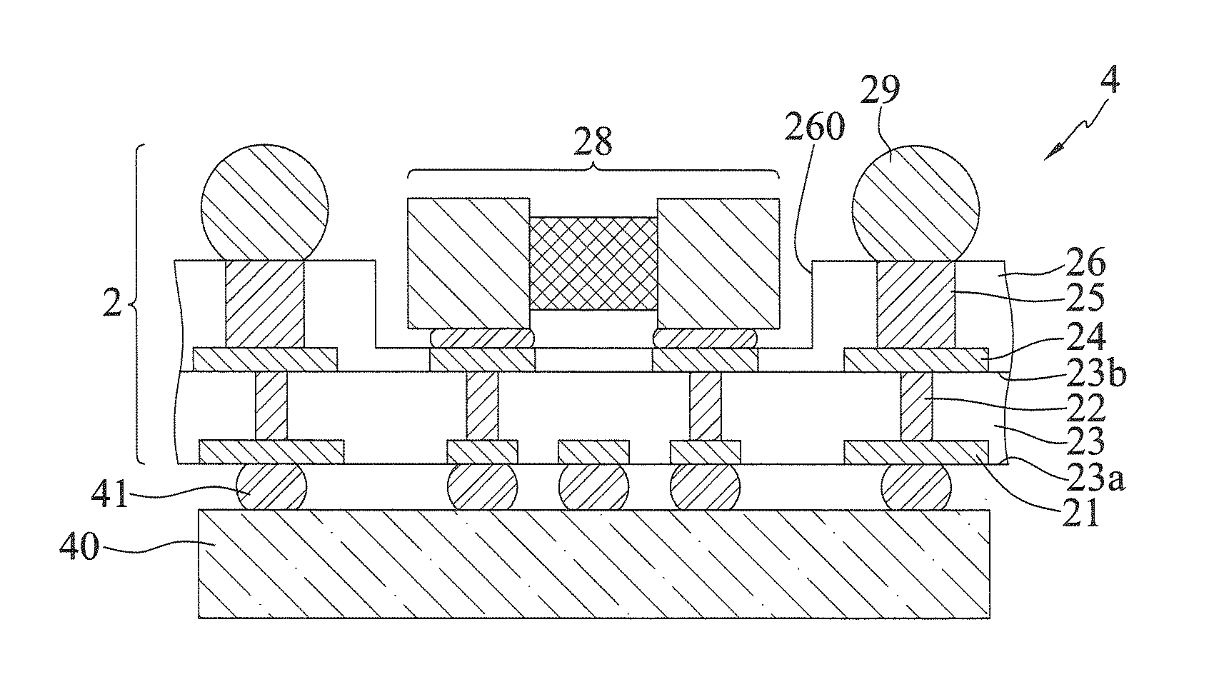
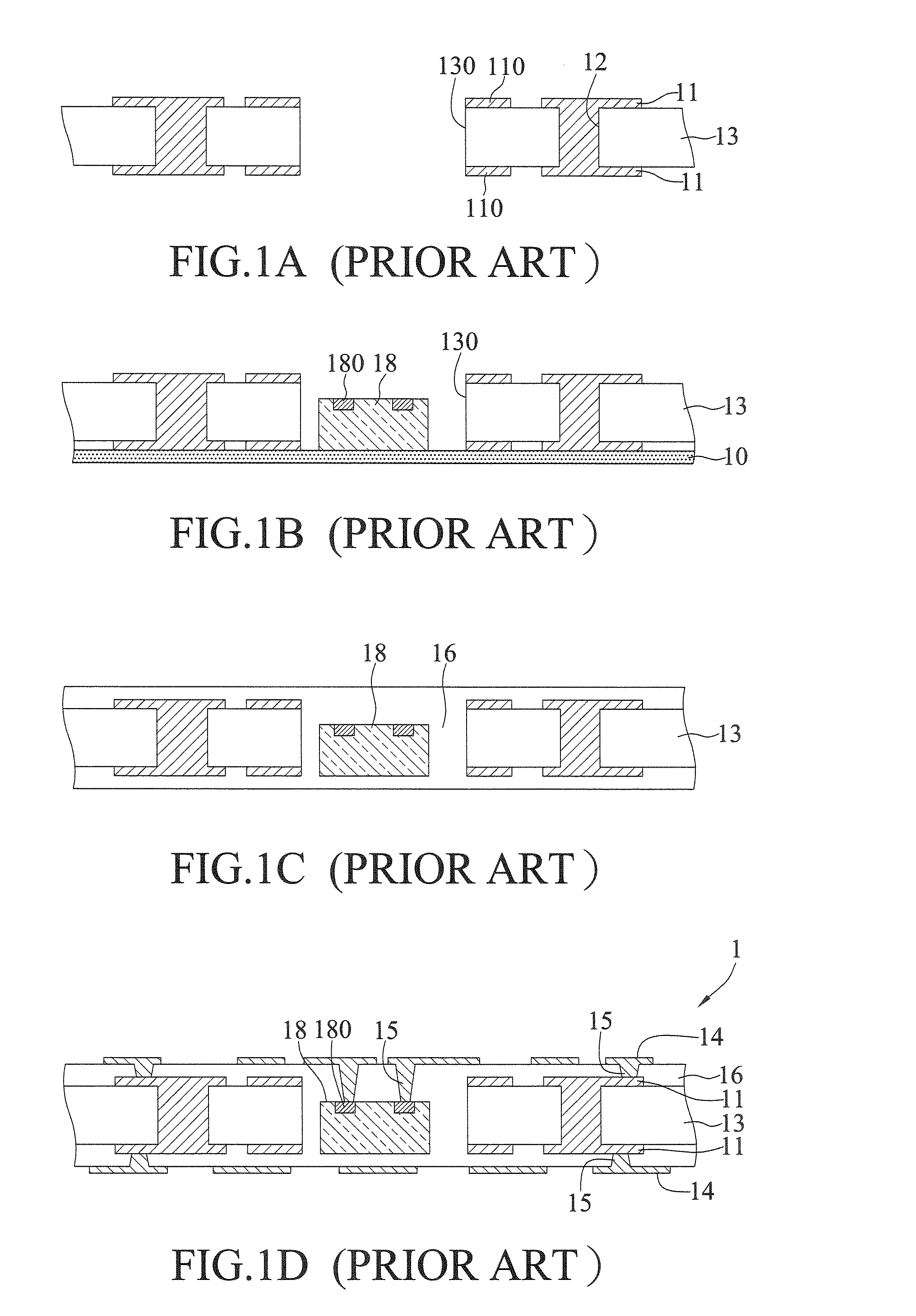
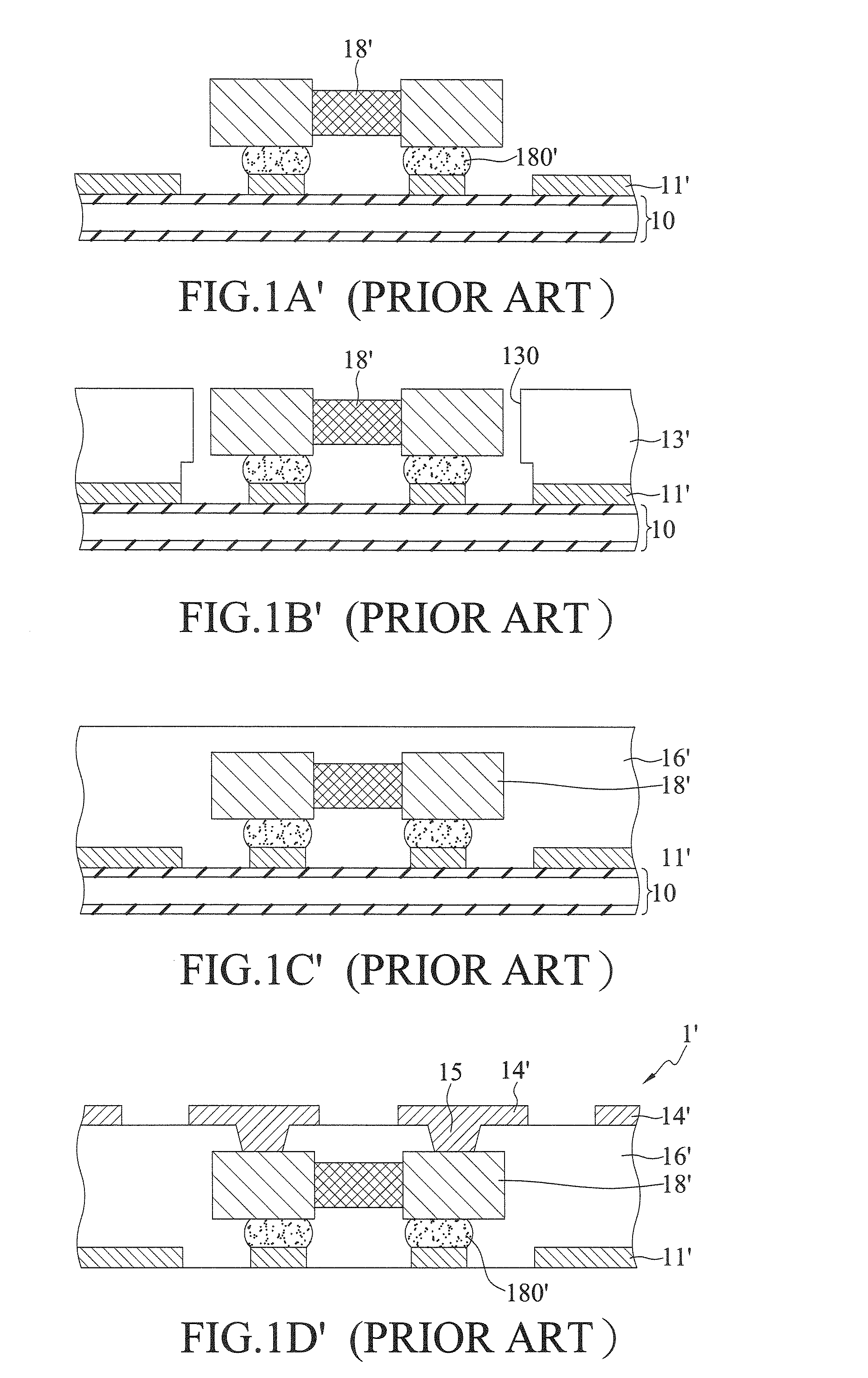
[0034]FIGS. 2A to 2F are cross-sectional view showing a method of manufacturing a package structure 2 according to the present invention.

[0035]As shown in FIG. 2A, a first wiring layer 21a is formed on a carrier board 20 by a patterning process, and a plurality of first conductors 22 are subsequently disposed on the first wiring layer 21.

[0036]In an embodiment...


PUM

PropertyMeasurementUnit
Structureaaaaaaaaaa
Electrical conductoraaaaaaaaaa
aaaaaaaaaa

Abstract

A method of manufacturing a package structure is provided, including forming a first wiring layer on a carrier board, forming up plurality of first conductors on the first wiring layer, forming a first insulating layer that encapsulates the first wiring layer and the first conductors, forming a second wiring layer on the first insulating layer, forming a plurality of second conductors on the second wiring layer, forming a second insulating layer that encapsulates the second wiring layer and the second conductors, and forming at least an opening on the second insulating layer for at least one electronic component to be disposed therein. Since the first and second insulating layers are formed before the opening, there is no need of stacking or laminating a substrate that already has an opening, and the electronic component will not be laminated and make a displacement. Therefore, the package structure thus manufactured has a high yield rate. The present invention further provides the package structure.

Description

BACKGROUND OF THE INVENTION[0001]1. Field of the Invention[0002]The present invention relates to package structures, and, more particularly, to a package structure for preventing electromagnetic interferences, and a method of manufacturing the package structure.[0003]2. Description of Related Art[0004]With the advancement in the technology of semiconductor package, different package structures have been developed to be incorporated in the smart phones, tablets, internet, laptops, and such semiconductor device is formed by mounting a chip on a package substrate such that the semiconductor chip is electrically connected thereto, and then followed by an encapsulating process to complete the formation of the semiconductor device. In addition, a package with an embedded chip which has the chip embedded in a package substrate is developed so as to reduce the overall thickness of the semiconductor package. Such semiconductor package is gaining popularity as it has the advantages of reduced...

Claims


Application Information

Patent Timeline
IPC IPC(8): H05K1/11H05K3/00H05K3/34H05K1/02H05K3/40H01L25/065H01L21/48H01L23/00H01L21/683H01L25/16H01L25/00H05K1/18H01L23/498
CPCH01L24/17Y10T29/49131H01L25/16H01L25/50H01L25/0657H05K2201/09036H05K2201/09218H05K2201/09563H05K2201/10545H01L2221/68359H01L2224/16227H05K1/113H05K1/181H05K1/183H05K3/007H05K3/3436H05K1/0216H05K3/4038H05K3/0026H05K3/0044H01L23/49827H01L23/49838H01L21/486H01L24/81H01L21/6835H01L2221/68345H01L2224/131H01L2224/16235H01L2924/15153H01L2924/15331H01L2924/19041H01L2924/19042H01L2924/19043H01L2924/19105H01L23/50H01L23/5389H05K1/0231H05K3/0032H05K3/3431H05K3/4682H05K3/4697H01L24/16H01L2224/13023H01L2224/16237H01L2224/16238H01L2224/16113H01L2224/16112H01L2224/133H01L2224/1329H01L2924/014H01L2924/00014H05K2201/10H05K1/162H05K2201/1003H05K2201/10015H05K1/185H05K2201/10007H05K3/284H05K2201/10037
Inventor HSU, SHIH-PINGTSENG, CHAO-CHUNG
Owner PHOENIX PIONEER TECH
Why Eureka
Try Eureka