Semiconductor device and manufacturing method of the same

a technology of semiconductor devices and manufacturing methods, applied in semiconductor devices, basic electric elements, electrical appliances, etc., can solve the problems of undesirable complexity of gate insulating films and manufacturing processes, reduce channel mobility, and reduce gate leakage current. , the effect of reducing the channel mobility

Active Publication Date: 2016-01-14
TOYODA GOSEI CO LTD
View PDF6 Cites 9 Cited by
  • Summary
  • Abstract
  • Description
  • Claims
  • Application Information

AI Technical Summary

Benefits of technology

[0008]The technique of JP 2008-103408A has a problem that formation of a nitride film by ALD requires higher plasma energy than formation of an oxide film and thereby rather decreases the channel mobility, in the case that the gate insulating film is formed by ALD in order to improve the film quality of the gate insulating film. The technique of JP 2013-74069A, on the other hand, has a problem that formation of the p-type semiconductor between the upper insulating film and the lower insulating film undesirably complicates the structure of the gate insulating film and the manufacturing process. There is accordingly a need to provide a technique that improves the carrier mobility and reduces the gate leakage current in the GaN-based MOSFET. With respect to the semiconductor device and the manufacturing method of the same, there are other needs including downsizing, cost reduction, resource saving, easy manufacture, improvement of convenience and improvement of durability.

Problems solved by technology

The technique of JP 2008-103408A has a problem that formation of a nitride film by ALD requires higher plasma energy than formation of an oxide film and thereby rather decreases the channel mobility, in the case that the gate insulating film is formed by ALD in order to improve the film quality of the gate insulating film.
The technique of JP 2013-74069A, on the other hand, has a problem that formation of the p-type semiconductor between the upper insulating film and the lower insulating film undesirably complicates the structure of the gate insulating film and the manufacturing process.

Method used


Image

  • Semiconductor device and manufacturing method of the same
  • Semiconductor device and manufacturing method of the same
  • Semiconductor device and manufacturing method of the same

Examples


first embodiment

A. First Embodiment

A-1. Structure of Semiconductor Device

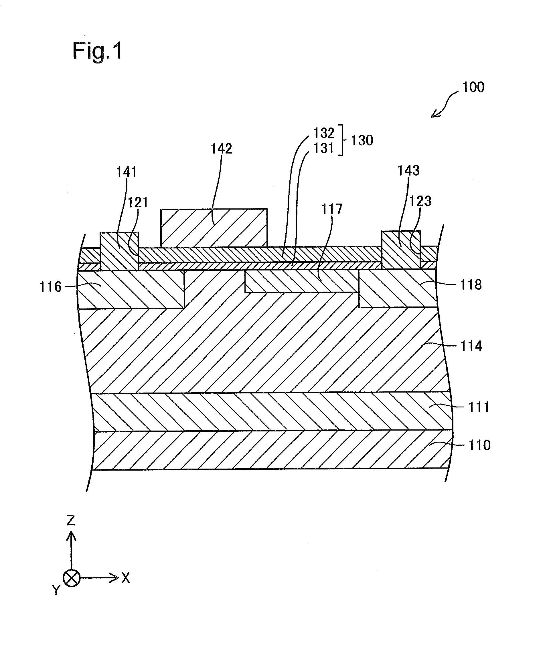
[0038]FIG. 1 is a sectional view schematically illustrating the structure of a semiconductor device 100 according to a first embodiment. The semiconductor device 100 is a GaN-based semiconductor device formed by using gallium nitride (GaN). According to this embodiment, the semiconductor device 100 is a lateral MOSFET (metal oxide semiconductor field effect transistor). According to this embodiment, the semiconductor device 100 is used for power control and is also called power device.

[0039]XYZ axes orthogonal to one another are illustrated in FIG. 1. Among the XYZ axes in FIG. 1, the X axis is an axis going from the left side of the sheet surface to the right side of the sheet surface of FIG. 1; +X-axis direction is a direction going rightward on the sheet surface and −X-axis direction is a direction going leftward on the sheet surface. Among the XYZ axes in FIG. 1, the Y axis is an axis going from the front side of the sheet...

second embodiment

B. Second Embodiment

B-1. Structure of Semiconductor Device

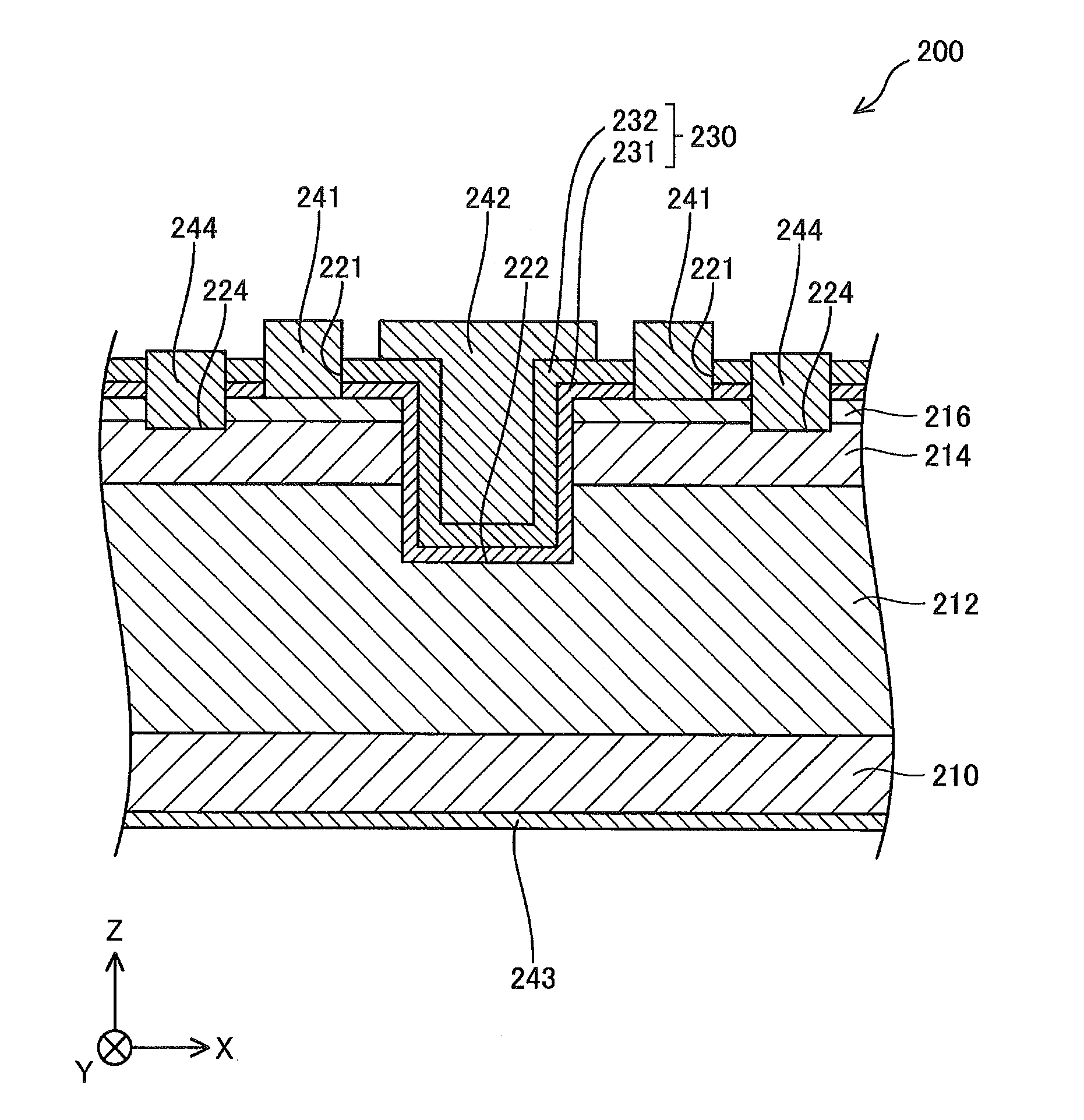
[0087]FIG. 3 is a sectional view schematically illustrating the structure of a semiconductor device 200 according to a second embodiment. The semiconductor device 200 is a GaN-based semiconductor device formed by using gallium nitride (GaN). According to this embodiment, the semiconductor device 200 is a vertical trench MOSFET. According to this embodiment, the semiconductor device 200 is used for power control and is also called power device. Like FIG. 1, XYZ axes are illustrated in FIG. 3.

[0088]The semiconductor device 200 includes a substrate 210, a semiconductor layer 212, a semiconductor layer 214 and a semiconductor layer 216. The semiconductor device 200 has a trench 222 and recesses 224 as features formed in these semiconductor layers 212, 214 and 216. Additionally, the semiconductor device 200 includes a gate insulating film 230, source electrodes241, a gate electrode 242, a drain electrode 243 and body electrodes 24...


PUM


Abstract

A semiconductor device, comprises: a semiconductor layer, a first gate insulating film, a second gate insulating film and a gate electrode. The semiconductor layer is mainly made of gallium nitride (GaN). The first gate insulating film is formed on the semiconductor layer by atomic layer deposition using ozone as an oxidizing agent and is mainly made of an oxide. The second gate insulating film is formed on the first gate insulating film by atomic layer deposition using oxygen plasma as an oxidizing agent, and is mainly made of an oxide and contains carbon (C) at a lower concentration than that in the first gate insulating film. The gate electrode is formed on the second gate insulating film.

Description

CROSS-REFERENCE TO RELATED APPLICATION[0001]The present application claims priority from Japanese patent application P2014-140520 filed on Jul. 14, 2014, the entirety of disclosures of which is hereby incorporated by reference into this application.BACKGROUND[0002]1. Technical Field[0003]The present invention relates to a semiconductor device and a manufacturing method of the same.[0004]2. Related Art[0005]MOSFETs (metal oxide semiconductor field effect transistors) using a semiconductor mainly made of gallium nitride (GaN) are known as semiconductor devices (semiconductor elements). This GaN-based MOSFET includes a semiconductor layer mainly made of GaN, a gate insulating film formed on the semiconductor layer and a gate electrode formed on the gate insulating film. The MOSFET is required to ensure sufficient channel mobility and reduce gate leakage current. The channel mobility denotes the mobility of a carrier moving through a channel area of the semiconductor layer. The gate lea...

Claims


Application Information

Patent Timeline
Patent Type & Authority Applications(United States)
IPC IPC(8): H01L29/423H01L21/02H01L21/28H01L21/306H01L29/20H01L29/51H01L29/66H01L29/78
CPCH01L29/42364H01L29/2003H01L29/511H01L29/4236H01L29/78H01L29/66446H01L21/30612H01L21/0228H01L21/28264H01L29/517H01L21/02126H01L21/022H01L21/02274H01L29/513H01L29/66522H01L29/66734H01L29/7813H01L29/7835
Inventor MURAKAMI, NORIAKIOKA, TOHRU
Owner TOYODA GOSEI CO LTD
Why Eureka
Try Eureka