Eureka AIR delivers breakthrough ideas for toughest innovation challenges, trusted by R&D personnel around the world.

Cleaning composition for semiconductor substrate and cleaning method

a technology for cleaning compositions and semiconductor substrates, applied in detergent compositions, detergent mixture preparations, detergent compounding agents, etc., can solve the problems of difficult removal of fine particles and/or attached particles between the pattern walls

Inactive Publication Date: 2016-02-04
JSR CORPORATIOON
View PDF14 Cites 7 Cited by
  • Summary
  • Abstract
  • Description
  • Claims
  • Application Information

AI Technical Summary

Benefits of technology

The present invention provides a cleaning composition for semiconductor substrates that can efficiently remove particles and easily remove the formed film. This composition can be used in manufacturing processes of semiconductor elements that require miniaturization and increased aspect ratio in the future.

Problems solved by technology

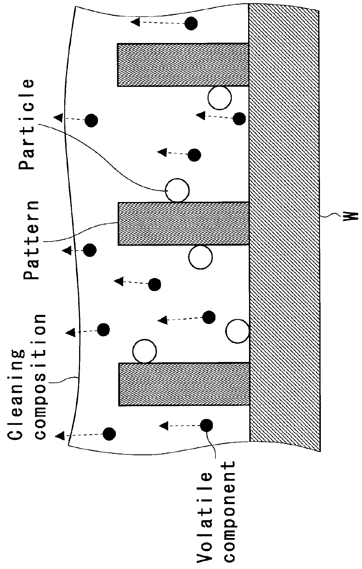
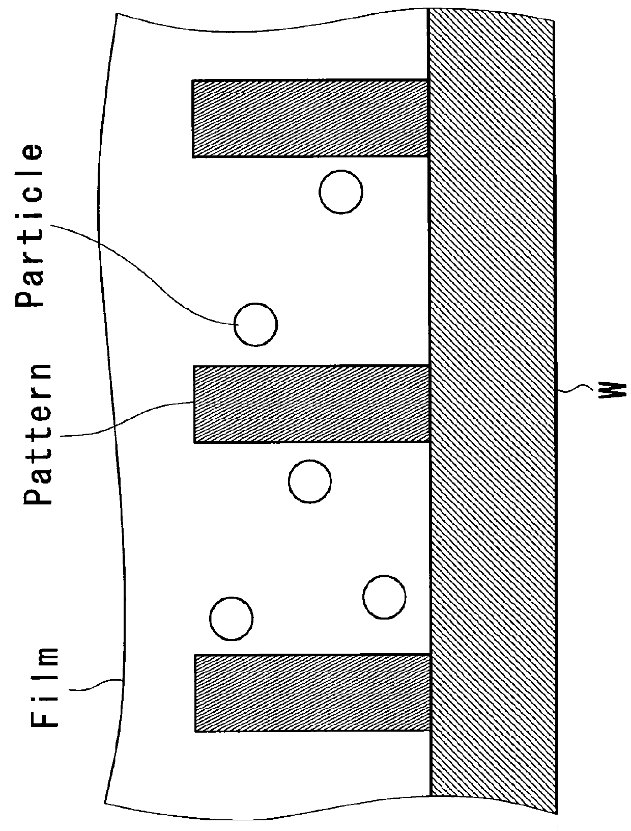
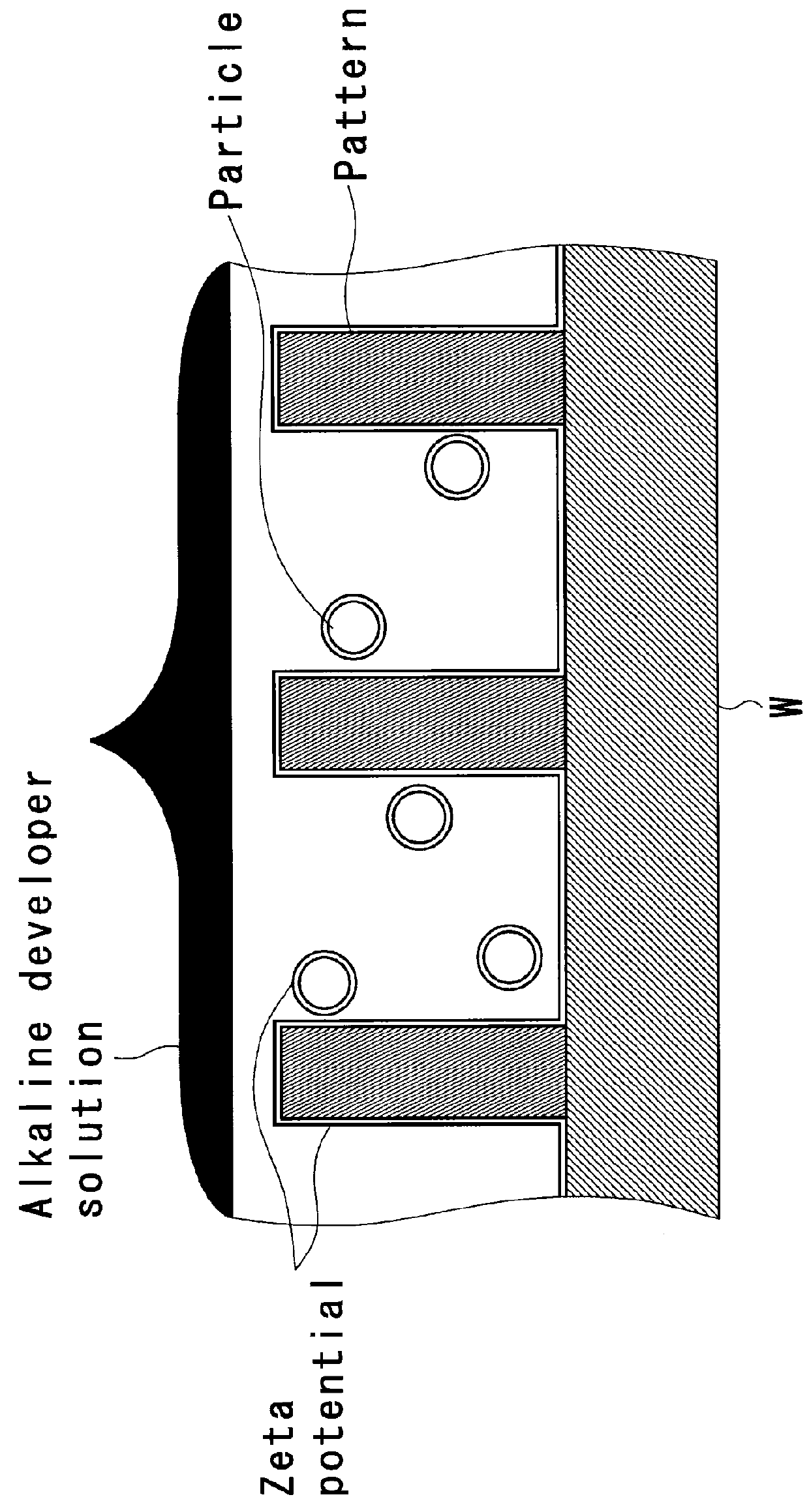
In cleaning through using a liquid and / or gas, it is difficult to achieve the flow of the liquid and / or gas between the pattern walls in the vicinity of a substrate surface, thereby making removal of fine particles and / or the attached particles between the pattern walls difficult.

Method used


Image

  • Cleaning composition for semiconductor substrate and cleaning method
  • Cleaning composition for semiconductor substrate and cleaning method
  • Cleaning composition for semiconductor substrate and cleaning method

Examples


production example 1

[0117]A monomer solution was prepared in which 100 g (100 mol %) of the compound (M-1) and 7.29 g (7 mol %) of azobisisobutyronitrile (AIBN) were dissolved in 100 g of 2-butanone. A 1,000 mL three-neck flask charged with 100 g of 2-butanone was purged with nitrogen for 30 min. The nitrogen purge was followed by heating to 80° C., and the monomer solution was added dropwise with stirring over 3 hrs using a dropping funnel. The time of the start of the dropwise addition was regarded as the time of the start of the polymerization reaction, and the polymerization was allowed for 6 hrs. After completing the polymerization, the reaction solution was cooled to no greater than 30° C. The reaction solution was concentrated in vacuo to give a mass of 150 g, and thereto were charged 150 g of methanol and 750 g of n-hexane to permit separation. After the separation, the underlayer liquid was recovered. To the recovered underlayer liquid was charged 750 g of n-hexane, and again purified through ...

production examples 2 to 22

[0118]Polymers (P-2) to (P-22) were synthesized in a similar manner to Production Example 1 except that the compound used and the combination were changed as shown in Table 1.

TABLE 1MonomerWeight averageDispersitycompositionYieldmolecularindexPolymertyperatio (mol %)(%)weight (Mw)(Mw / Mn)Production Example 1P-1M-11008010,5001.52Production Example 2P-2M-21007910,4001.51Production Example 3P-3M-31008010,0001.55Production Example 4P-4M-4 / M-570 / 308010,5201.53Production Example 5P-5M-1 / M-690 / 10819,9001.50Production Example 6P-6M-4 / M-680 / 207810,2001.51Production Example 7P-7M-6 / M-850 / 507910,4501.52Production Example 8P-8M-3 / M-670 / 308210,0001.52Production Example 9P-9M-1 / M-950 / 50847,4001.35Production Example 10P-10M-1 / M-1060 / 408310,3001.52Production Example 11P-11M-6 / M-1140 / 607811,0001.51Production Example 12P-12M-6 / M-1240 / 60829,8001.50Production Example 13P-13M-6 / M-1340 / 60839,5001.53Production Example 14P-14M-1 / M-1460 / 40829,9001.52Production Example 15P-15M-6 / M-1560 / 408110,3001.55Productio...

example 1

[0119]The polymer (P-1) in an amount of 100 parts by mass, and 7,400 parts by mass of 4-methyl-2-pentanol (MIBC) were mixed to prepare a homogenous solution. This solution was filtered through a filter made of high density polyethylene (HDPE) (pore size: 5 nm, PhotoKleen EZD, manufactured by Japan Pall Corporation). A decrease of the particles having a diameter of no greater than 150 μm in the liquid to 10 particles / mL was ascertained by Liquld-Borne Particle Sensor (KS-41B, manufactured by Rion Co., Ltd.), and thus a cleaning composition (D-1) was prepared. The solid content concentration was about 1.5% by mass.


PUM

PropertyMeasurementUnit
Temperatureaaaaaaaaaa
Percent by massaaaaaaaaaa

Abstract

A cleaning composition for a semiconductor substrate contains a solvent, and a polymer that includes a fluorine atom, a silicon atom or a combination thereof. The content of water in the solvent is preferably no greater than 20% by mass. The cleaning composition preferably further contains an organic acid which is a non-polymeric acid. The organic acid is preferably a polyhydric carboxylic acid. The acid dissociation constant of the polymer is preferably less than that of the organic acid. The solubility of the organic acid in water at 25° C. is preferably no less than 5% by mass. The organic acid is preferably a solid at 25° C.

Description

CROSS-REFERENCE TO RELATED APPLICATIONS[0001]The present application claims priority to Japanese Patent Application No. 2014-157071, filed Jul. 31, 2014. The contents of this application are incorporated herein by reference in their entirety.BACKGROUND OF THE INVENTION[0002]1. Field of the Invention[0003]The present invention relates to a cleaning composition for a semiconductor substrate and a cleaning method.[0004]2. Discussion of the Background[0005]In production processes of semiconductor substrates, cleaning is conducted in order to remove contaminants such as particles attached onto the surface of the substrates having a pattern formed thereon. In recent years, miniaturization of the formed pattern, and an increase of the aspect ratio have advanced. In cleaning through using a liquid and / or gas, it is difficult to achieve the flow of the liquid and / or gas between the pattern walls in the vicinity of a substrate surface, thereby making removal of fine particles and / or the attac...

Claims


Application Information

Patent Timeline
IPC IPC(8): C11D11/00
CPCC11D11/0058C11D11/0047C11D3/373C11D7/50C11D2111/42C11D2111/22B08B7/0014C08F120/18C08F120/24C08F120/28C08F132/08C08K5/092C11D3/2086C11D3/245C11D3/43H01L21/02052
Inventor MOCHIDA, KENJISHIMA, MOTOYUKI
Owner JSR CORPORATIOON
Why Eureka
Eureka Blog
Learn More