Method for improving adhesion between porous low k dielectric and barrier layer

Active Publication Date: 2016-02-18
SEMICON MFG INT (SHANGHAI) CORP
View PDF5 Cites 5 Cited by
  • Summary
  • Abstract
  • Description
  • Claims
  • Application Information

AI Technical Summary

Benefits of technology

[0015]The following description, together with the accompanying drawings, will pro

Problems solved by technology

However, in the conventional process, the interface surface between the porous low-k dielectric layer and the diffusion barrier layer is rough, leading to poor adhesio

Method used


Image

  • Method for improving adhesion between porous low k dielectric and barrier layer
  • Method for improving adhesion between porous low k dielectric and barrier layer
  • Method for improving adhesion between porous low k dielectric and barrier layer

Examples


embodiment 1

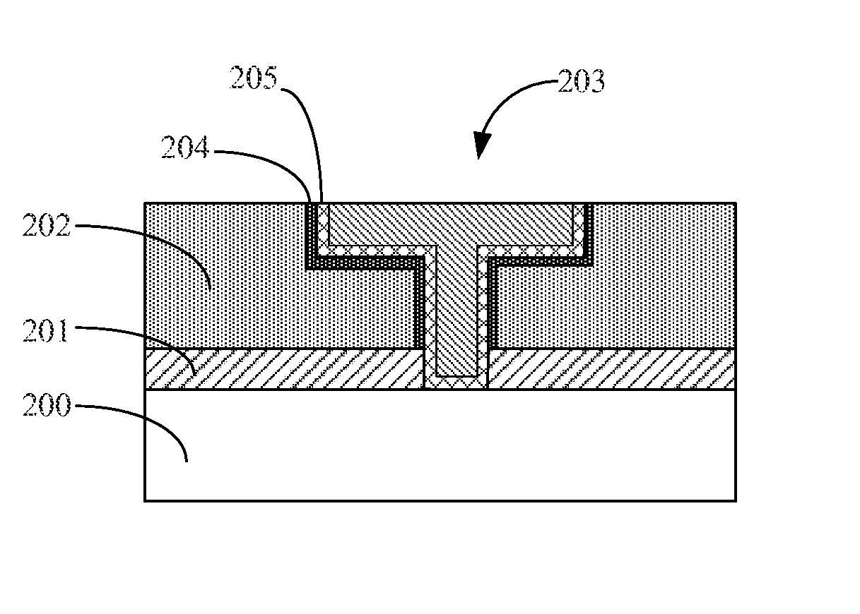
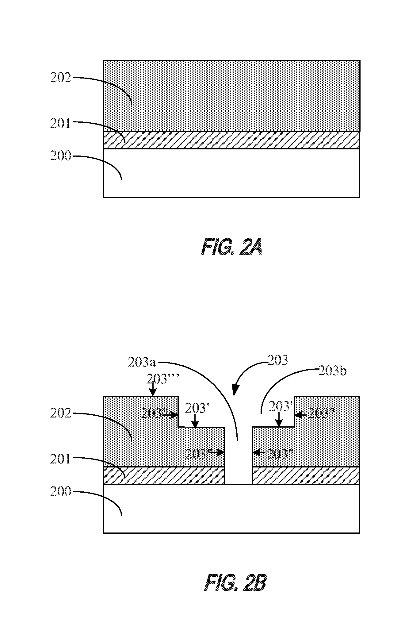
[0030]FIGS. 2A through 2F are simplified cross-sectional views illustrating stages of process steps of forming a semiconductor device according to an embodiment of the present invention.

[0031]Referring to FIG. 2A, a semiconductor substrate 200 is provided. Semiconductor substrate 200 can be made of undoped silicon, doped silicon, silicon on insulator (SOI) and the like. By way of an example, semiconductor substrate 200 includes a monocrystalline silicon material. One or more isolation structures and well structures may be formed in semiconductor substrate 200, which are not shown herein for the sake of clarity.

[0032]One or more front-end devices may be formed on semiconductor substrate 200, which are not shown herein for the sake of clarity. The term “front-end” device is referred to herein as a semiconductor device structure before the back-end-of-the line (BEOL). The term front-end device is not intended to limit the semiconductor device structure to a particular form disclosed.

[0...

embodiment 2

[0059]FIG. 4 is a cross-sectional view illustrating a semiconductor device structure 40 according to an embodiment of the present invention. Semiconductor device structure 40 includes: a semiconductor substrate 400; a porous low-k dielectric layer 402 disposed on semiconductor substrate 400. In an embodiment, an etch stop layer 401 may be disposed between semiconductor substrate 400 and porous low-k dielectric layer 402. Semiconductor substrate 400 may be of an undoped silicon, doped silicon, silicon on insulator, and the like. By way of example, semiconductor substrate 400 is made of a monocrystaline silicon. Semiconductor substrate 400 may include isolation structures and various well structures, which are not shown for the sake of clarity. Semiconductor substrate 400 may include one or more front-end devices (not shown) formed thereon. A front-end device is referred to a semiconductor structure that has not gone through the back-end-of-the line (BEOL) process.

[0060]Etch stop laye...

embodiment 3

[0065]Embodiments of the present invention provide an electronic device including a semiconductor device that is manufactured by the above-described method of embodiment 1 or the above-described device structure of embodiment 2.

[0066]In accordance with the present invention, the electronic device may be a mobile phone, a laptop computer, a netbook, a tablet PC, a game console, a TV, a DVD player, a GPS device, a camera, a voice recorder, MP3, MP4, PSP players, and other semiconductor devices including intermediate products and electronic components that are manufactured using the above-described method to improve reliability and yield.


PUM


Abstract

A semiconductor device and method for manufacturing the same are provided. The method includes providing a semiconductor substrate, forming a porous low-k dielectric layer on the semiconductor substrate, forming a through-hole and a trench of a copper interconnect structure, performing a helium plasma treatment on an exposed surface of the porous low-k dielectric layer, performing a nitrogen plasma treatment on the exposed surface of the porous low-k dielectric layer to form a silicon nitride layer, performing an argon plasma treatment on the silicon nitride layer, and forming a diffusion barrier layer on bottoms and sidewalls of the through-hole and the trench of the copper interconnect structure. Through the successive helium, nitrogen and argon plasma treatments, the low-k dielectric layer has a smooth and dense surface that increases the adhesion strength between the low-k dielectric layer and the diffusion barrier layer to improve reliability and yield of the semiconductor device.

Description

CROSS-REFERENCES TO RELATED APPLICATIONS[0001]This application claims priority to Chinese patent application No. 201410398110.8, filed Aug. 13, 2014, the content of which is incorporated herein by reference in its entirety.BACKGROUND OF THE INVENTION[0002]The present invention relates to a semiconductor structure and method of manufacture, and more particularly to a semiconductor device and manufacturing method thereof.[0003]With the continuous decrease of semiconductor feature sizes, capacitive crosstalk between metal interconnect layers has a significant impact on semiconductor device performance. The use of a porous low-k dielectric layer disposed between metal interconnect layers is a good way to solve the problem of capacitive crosstalk.[0004]The number of metal interconnect layers in a logic circuit of a semiconductor device may range from a few to more than 10 layers, each of the metal interconnect layers forms a respective layer of a metal interconnect structure. Referring t...

Claims


Application Information

Patent Timeline
IPC IPC(8): H01L21/768H01L23/522H01L23/532
CPCH01L21/76843H01L21/76814H01L23/5226H01L23/53238H01L21/76861H01L21/76826H01L21/76831H01L23/5329H01L23/53295H01L2924/0002H01L2924/00H01L21/02203H01L21/76802H01L21/7684H01L21/76877
Inventor ZHOU, MING
Owner SEMICON MFG INT (SHANGHAI) CORP
Why Eureka
Try Eureka